MAXIMUM RATINGS
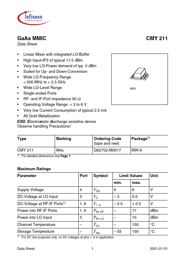
Parameter Port Symbol Limit Values min. Supply Voltage DC-Voltage at LO Input DC-Voltage at RF-IF Ports1) Power into RF-IF Ports Power into LO Input Channel Temperature Storage Temperature 1) Unit max. 6 0.5 + 0.5 17 10 150 150 V V V dBm dBm 4 3 1, 6 1, 6 3 – – VDD V3 V1, 6 PIN, RF PIN, LO TCh Tstg 0 –3 – 0.5 – – – – 55 °C °C For DC test purposes only, no DC voltages at pins 1, 6 in application. Data Sheet 1 2001-01-01 GaAs Components CMY 211 Thermal Resistance Parameter Channel to Soldering Point (GND) Symbol Value Unit K/W RthChS ≤ 100 ELECTRICAL CHARACTERISTICS
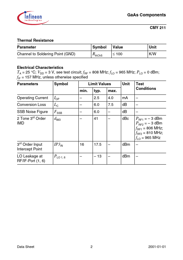
TA = 25 °C; VDD = 3 V, see test circuit; fRF = 808 MHz; fLO = 965 MHz; PLO = 0 dBm; fIF = 157 MHz, unless otherwise specified Parameters Symbol min. Operating Current Conversion Loss SSB Noise Figure 2 Tone 3rd Order IMD Limit Values typ. 2.5 6.0 6.0 41 max. 4.0 7.5 – – mA dB dB dBc Unit Test Conditions – – – IOP LC FSSB dIM3 – – – – PRF1 = – 3 dBm PRF2 = – 3 dBm fRF1 = 806 MHz; fRF2 = 810 MHz; fLO = 965 MHz –... Infineon Technologies