Datasheet Summary
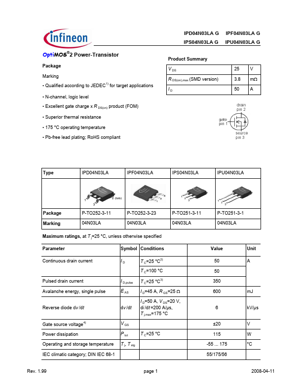
Type
OptiMOS®2 Power-Transistor
Package Marking
- Qualified according to JEDEC1) for target applications
- N-channel, logic level
- Excellent gate charge x R DS(on) product (FOM)
- Superior thermal resistance
- 175 °C operating temperature
- Pb-free lead plating; RoHS pliant
IPD04N03LA G IPF04N03LA G IPS04N03LA G IPU04N03LA G
Product Summary V DS R DS(on),max (SMD version) ID
25 V 3.8 mΩ 50 A
Type
IPF04N03LA
IPS04N03LA
IPU04N03LA
Package Marking
P-TO252-3-11 04N03LA
P-TO252-3-23 04N03LA
P-TO251-3-11 04N03LA
P-TO251-3-1 04N03LA
Maximum ratings, at T j=25 °C, unless otherwise specified
Parameter
Symbol Conditions
Continuous drain current
T C=25...