IPD320N20N3G
IPD320N20N3G is Power-Transistor manufactured by Infineon.
Features
- N-channel, normal level
- Excellent gate charge x R DS(on) product (FOM)
- Very low on-resistance R DS(on)
- 175 °C operating temperature
- Pb-free lead plating; Ro HS pliant
- Qualified according to JEDEC1) for target application
- Halogen-free according to IEC61249-2-21
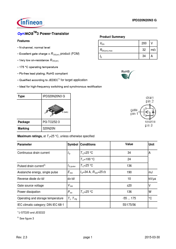
Product Summary V DS R DS(on),max ID 200 32 34 V mΩ A
- Ideal for high-frequency switching and synchronous rectification Type IPD320N20N3 G
Package Marking
PG-TO252-3 320N20N
Maximum ratings, at T j=25 °C, unless otherwise specified Parameter Continuous drain current Symbol Conditions ID T C=25 °C T C=100 °C Pulsed drain current2) Avalanche energy, single pulse Gate source voltage Power dissipation Operating and storage temperature IEC climatic category; DIN IEC 68-1
1) 2)
Value 34 24 136 190 ±20
Unit A
I D,pulse E AS V GS P tot T j, T stg
T C=25 °C I D=34 A, R GS=25 Ω m J V W °C
T C=25 °C
136 -55 ... 175 55/175/56
J-STD20 and JESD22 See figure 3
Rev. 2.2 page 1
2009-10-22
IPD320N20N3 G
Parameter
Symbol Conditions min.
Values typ. max.
Unit
Thermal characteristics Thermal resistance, junction
- case Thermal resistance, junction ambient R th JC R th JA minimal footprint 6 cm2 cooling area 3) 1.1 75 50 K/W
Electrical characteristics, at T j=25 °C, unless otherwise specified Static characteristics Drain-source breakdown voltage Gate threshold voltage Zero gate voltage drain current V (BR)DSS V GS=0 V, I D=1 m A V GS(th) I DSS V DS=V GS, I D=90 µA V DS=160 V, V GS=0 V, T j=25 °C V DS=160 V, V GS=0 V, T j=125 °C Gate-source leakage current Drain-source on-state resistance Gate resistance Transconductance I GSS R DS(on) RG g fs |V DS|>2|I D|R DS(on)max, I D=34 A V GS=20 V, V DS=0 V V GS=10 V, I D=34 A 200 2 3 0.1 4 1 µA V
10 1 27 2.5 55
100 100 32 n A mΩ Ω S
2 Device on 40 mm x 40 mm x 1.5 mm epoxy PCB FR4 with 6 cm (one layer, 70 µm thick) copper area for drain connection. PCB is vertical in still air.
3)
Rev. 2.2 page 2
2009-10-22
IPD320N20N3...