PXAC261002FC Overview
Key Specifications
Description
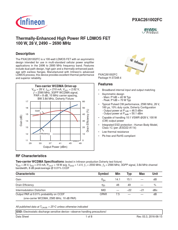
The PXAC261002FC is a 100-watt LDMOS FET with an asymmetric design intended for use in multi-standard cellular power amplifier applications in the 2496 to 2690 MHz frequency band. Features include dual-path design, high gain and a thermally-enhanced package with earless flanges.
Key Features
- Broadband internal input and output matching
- Asymmetric design
- Main: P1dB = 40 W Typ
- Peak: P1dB = 70 W Typ