Infineon Technologies S70GL02GS
The S70GL02GS 2-Gb MIRRORBIT™ flash memory device is fabricated on 65-nm MIRRORBIT™ process technology. This device offers a fast page access time of 25 ns with a corresponding random access time of 110 ns. It features a write buffer that allows a maximum of 256 words/512 bytes to be programmed in one operation, resulting in faster effective programming time than standard single byte/word programming algorithms.| Part No. | S70GL02GS |
|---|---|
| Datasheet | S70GL02GS Download |
| Manufacturer |  Infineon Technologies |
| Description | 2Gbit (256MB) GL-S Flash |
| Buy | Stock & Price |
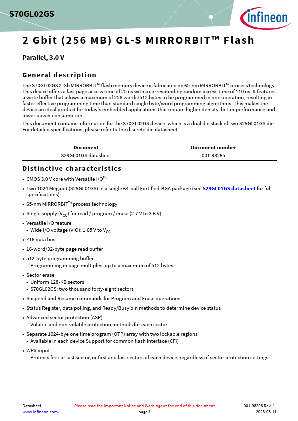
S70GL02GS 2 Gbit (256 MB) GL-S MIRRORBIT™ Flash Parallel, 3.0 V General description This makes the device an ideal product for today’s embedded applications that require higher density, better performance and lower power consumption. This document contains information for the S70GL02GS device, which is a dual die stack of two S29GL01GS die. For detailed specifications, please refer to the discrete die datasheet. Document S29GL01GS datasheet Document number 001-98285 Distinctive characteristics
● CMOS 3.0 V core with Versatile I/O™
● Two 1024 Megabit (S29GL01GS) in a single 64-ball Fortified-BGA package (see S29GL01GS datasheet for full specifications)
● 65-nm MIRRORBIT™ process technology
● Single supply (VCC) for read / program / erase (2.7 V to 3.6 V)
● Versatile I/O feature - Wide I/O voltage (VIO): 1.65 V to VCC
● ×16 data bus
● 16-word/32-byte page read buffer
● 512-byte programming buffer - Programming in page multiples, up to a maximum of 512 bytes
● Sector erase - Uniform 128-K...