Infineon Technologies SIPC42S2N08
The information herein is given to describe certain components and shall not be considered as warranted characteristics.| Part No. | SIPC42S2N08 |
|---|---|
| Datasheet | SIPC42S2N08 Download |
| Manufacturer |  Infineon Technologies |
| Description | OptiMOS Chip data sheet |
| Buy | Stock & Price |
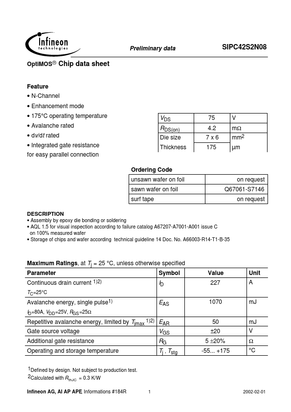
DESCRIPTION
● Assembly by epoxy die bonding or soldering● AQL 1.5 for visual inspection according to failure catalog A67207-A7001-A001 issue C on 100% measured wafer
● Storage of chips and wafer according technical guideline 14 Doc. No. A66003-R14-T1-B-35 VDS RDS(on) Die size Thickness 75 4.2 7x6 175 V mΩ mm2 µm on request Q67061-S7146 on request
MAXIMUM RATINGS
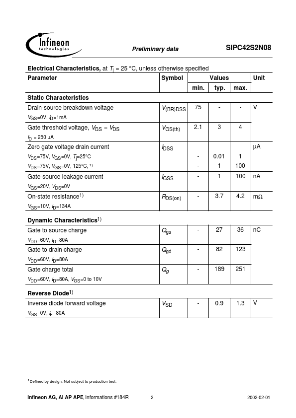
, at Tj = 25 °C, unless otherwise specified Parameter Continuous drain current 1)2) TC=25°C Symbol ID EAS Value 227 1070 50 ±20 5 ±20% -55... +175 Unit A mJ mJ V Ω °C Avalanche energy, single pulse1) ID =80A, VDD =25V, RGS =25Ω Repetitive avalanche energy, limited by Tjmax 1)2) EAR Gate source voltage VGS Additional gate resistance Operating and storage temperature 1Defined by design. Not subject to production test. 2Calculated with R = 0.3 K/W thJC RG Tj , Tstg Infineon AG, AI AP APE, Informations #184R 1 2002-02-01 Preliminary data SIPC42S2N08ELECTRICAL CHARACTERISTICS
, at Tj = 25 °C, unless otherwise specified Parameter Static Characteristics Drain-source breakdown voltage VGS =0V, ID =1mA Symbol min.