Infineon Technologies SPN02N60C3
Power Transistor
| Part No. | SPN02N60C3 |
|---|---|
| Datasheet | SPN02N60C3 Download |
| Manufacturer |  Infineon Technologies |
| Description | Power Transistor |
| Buy | Stock & Price |
MAXIMUM RATINGS
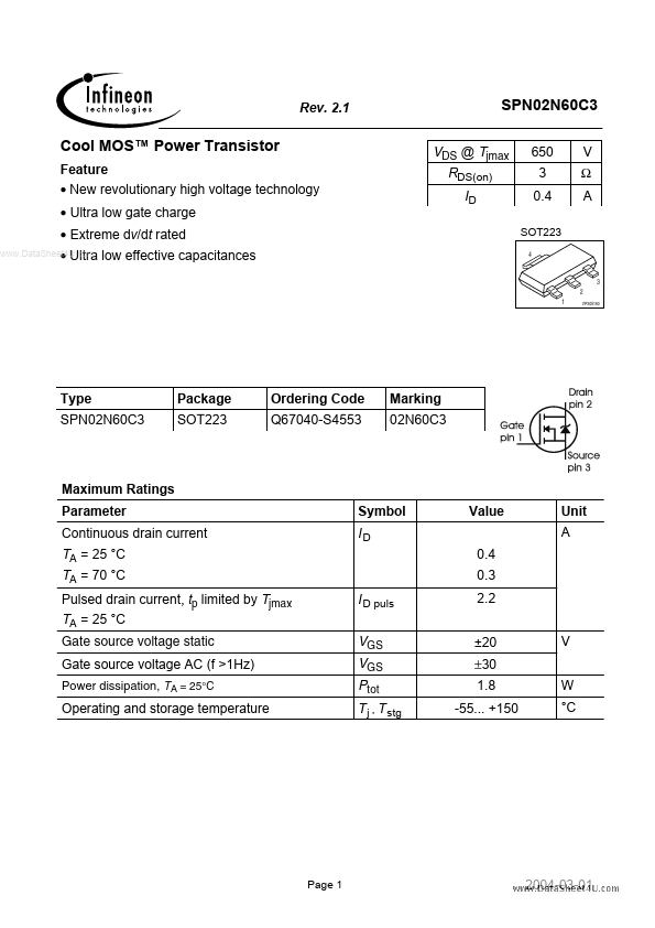
Parameter Symbol ID Value Unit Continuous drain current TA = 25 °C TA = 70 °C A 0.4 0.3 Pulsed drain current, tp limited by Tjmax TA = 25 °C Gate source voltage static I D puls VGS VGS Ptot T j , T stg 2.2 ±20 ±30 V W °C Gate source voltage AC (f >1Hz) Power dissipation, T A = 25°C 1.8 -55... +150 Operating and storage temperature Page 1 2004-03-01 Rev. 2.1 SPN02N60C3MAXIMUM RATINGS
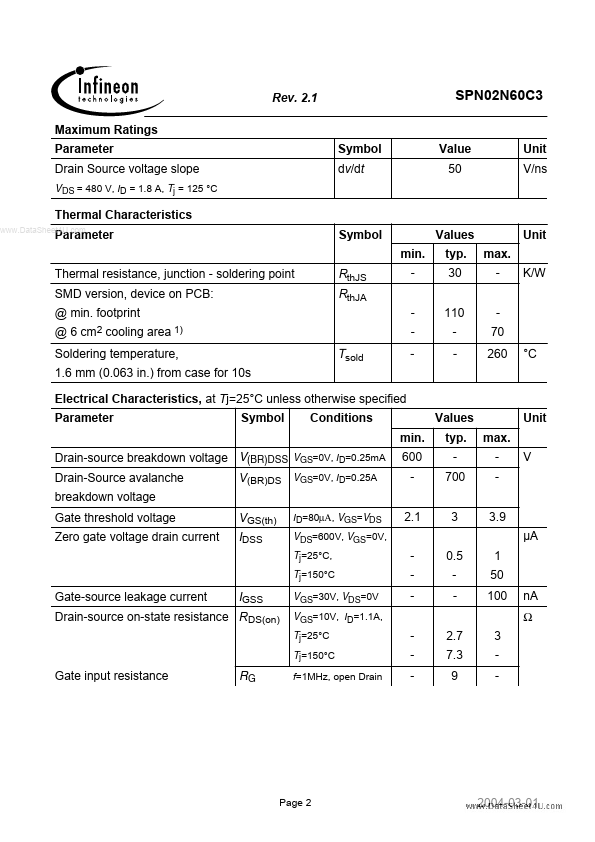
Parameter Drain Source voltage slope V DS = 480 V, ID = 1.8 A, Tj = 125 °C Symbol dv/dt Value 50 Unit V/ns Thermal Characteristics Parameter Thermal resistance, junction - soldering point SMD version, device on PCB: @ min. footprint @ 6 cm2 cooling area 1) Symbol min. RthJS RthJA - Values typ. 30 110 max. 70 Unit K/W Soldering temperature, 1.6 mm (0.063 in.) from case for 10s Tsold - - 260 °CELECTRICAL CHARACTERISTICS
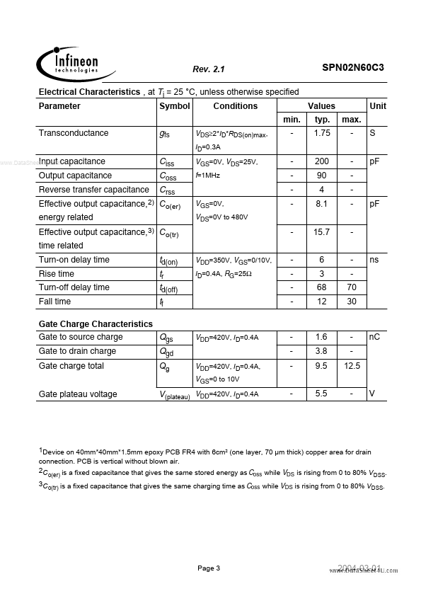
, at Tj=25°C unless otherwise specified Parameter Symbol Conditions min. Drain-source breakdown voltage V(BR)DSS VGS=0V, ID=0.25mA Drain-Source avalanche breakdown voltage Gate threshold voltage Zero gate voltage drain current VGS(th) IDSS ID=80µΑ, VGS=VDS VDS=600V, VGS=0V, Tj=25°C, Tj=150°C Values typ.