Datasheet Summary
CAN TRANSCEIVER
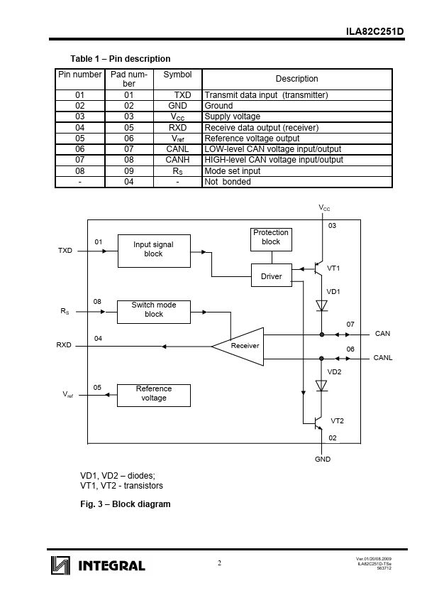
The INA82C251 is the interface between the CAN protocol controller and the physical bus.. The device provides differential transmit capability to the bus and differential receive capability to the CAN controller. The IC is intended for automotive electronic applications
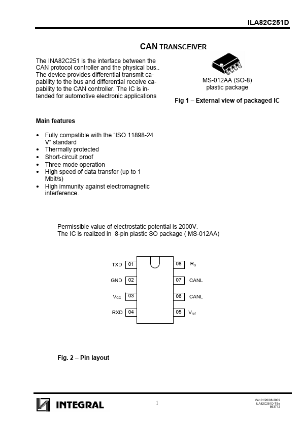
MS-012AA (SO-8) plastic package
Fig 1
- External view of packaged IC
Main Features
- Fully patible with the “ISO 11898-24 V” standard
- Thermally protected
- Short-circuit proof
- Three mode operation
- High speed of data transfer (up to 1
Mbit/s)
- High immunity against electromagnetic interference.
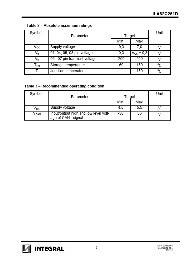
Permissible value of electrostatic potential is 2000V. The IC is realized in 8-pin...