ILE4270S
ILE4270S is POWER VOLTAGE REGULATOR manufactured by Integral.
- Part of the ILE4270G comparator family.
- Part of the ILE4270G comparator family.
ILE4270G, ILE4270S
ICS ILE4270G, ILE4270S OF POWER VOLTAGE REGULATOR
5 V/550MA WITH LOW RESIDUAL VOLTAGE
(FUNCTIONAL EQUVIVALENT TLE4270G BY SIEMENS)
ICs perform stabilizing of output voltage 5 V with 2% accuracy in the range of input voltages from
5.5 to 26 V, providing a load current not less 550 mA with residual voltage less than 0.7 V.
The spread of the output voltage is provided by adjustment of the reference voltage by means of fusion of diode jumpers on the crystal. Maximum input voltage 42 V (65 V during the time t ≤ 400 ms).
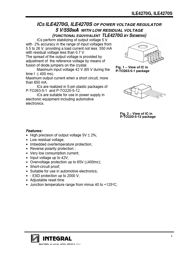
Fig. 1
- View of IC in P-TO263-5-1 package
Maximum output current when a short circuit, more than 650 mA.
ICs are realized in 5-pin plastic...