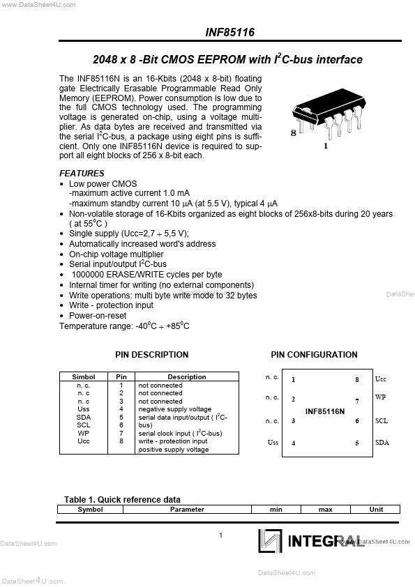
INF85116
Overview
- Low power CMOS -maximum active current 1.0 mA -maximum standby current 10 µA (at 5.5 V), typical 4 µA
- Non-volatile storage of 16-Kbits organized as eight blocks of 256x8-bits during 20 years ( at 55oC )
- Single supply (Ucc=2,7 ÷ 5,5 V);
- Automatically increased word's address
- On-chip voltage multiplier
- Serial input/output I2C-bus
- 1000000 ERASE/WRITE cycles per byte
- Internal timer for writing (no external components) DataShee
- Write operations: multi byte write mode to 32 bytes
- Write - protection input