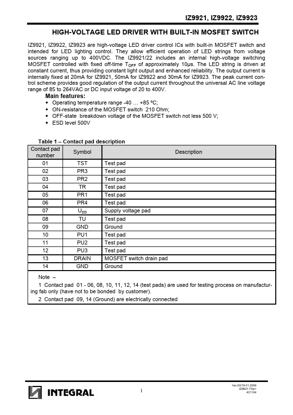
DESCRIPTION
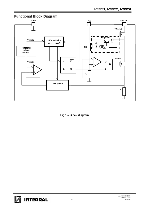
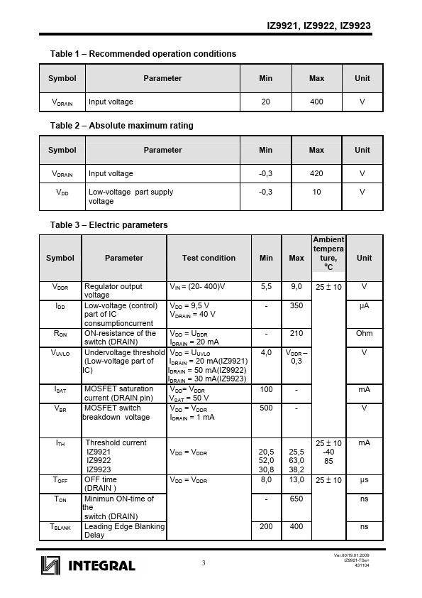
Note – 1 Contact pad 01 - 06, 08, 10, 11, 12, 14 (test pads) are used for testing process on manufacturing fab only (have not to be bonded by customer). 2 Contact pad 09, 14 (Ground) are electrically connected Ver.00/19.01.2009 1 IZ9921-TSe+ 431104 Functional Block Diagram GND VREF2 Reference voltage source VREF1 + RC-oscillator (TOFF = 10 µS) SQ RQ Delay line IZ9921, IZ9922, IZ9923 VDD DRAIN HVNMOS Regulator D1 D4 R1 D2 D3 - NMOS +& R2 R Fig 1 – Block diagram Ver.00/19.01.2009 2 IZ9921-TSe+ 431104 IZ9921, IZ9922, IZ9923 Table 1 – Recommended operation conditions Symbol Parameter Min Max Unit VDRAIN Input voltage Table 2 – Absolute maximum rating 20 400 V Symbol Parameter Min Max Unit VDRAIN VDD Input voltage Low-voltage part supply voltage -0,3 420 V -0,3 10 V Table 3 – Electric parameters Symbol Parameter Test condition Ambient tempera Min Max ture, Unit oC VDDR Regulator output voltage VIN = (20- 400)V 5,5 9,0 25 ± 10 IDD Low-voltage (control) VDD = 9,5 V part of IC VDRA... Integral