Description
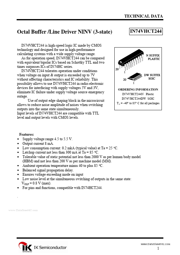
Input OUTPUT ENABLE Data input Data output Data input Data output Data input Data output Data input Data output Common output Data input Data output Data input Data output Data input Data output Data input Data output Input OUTPUT ENABLE Supply output from voltage source 01 02 03 04 05 06 07 08 09 10 02 03 04 05 06 07 08 09 10 11 12 13 14 15 16 17 18 19 20 2G VCC www.DataSheet4U.com 2 IN74VHCT244 Absolute maximum conditions* Parameter, unit Supply voltage, V Input voltage, V Output voltage, V Output voltage, V Input diode current, mA Current of common output and supply output, mA Output current, mA Output diode current, mA Dissipated power, mW Symbol VCC Vin Vout Vout1 Iik Icc Iout Iok Pd min -0.5 -0.5 -0.5 -0.5 Value max 7.0 7.0 VCC + 0.5B 7.0 -20 ±75 ±25 ±20 180 Under absolute maximum conditions operation of microcircuit is not guaranteed. Operation is guaranteed under maximum conditions Maximum conditions Parameter, unit Symbol min 4.5 0 0 0 0 Value max 5.5 VCC VCC 5.5* ±8.0 20 Supply voltage, V Input voltage,V Output voltage, V Output voltage, V Output current, mA Input rise and fall time, ns/V * - Outputs in the third state VCC Vin Vout Vout1 Iout tLH, tHL www.DataSheet4U.com 3 IN74VHCT244 DC electrical characteristics Value Symbo l VIH VIL VOH Parameter High input voltage Test conditions VCC, V 25 °C min 2.0 - 4.42 5.42 3.94 - - - max 0.8 - - - 0.09 0.09 0.36 ±0.25 ±0.1 ±0.1 4.0 1.35 -40 to 85 °C min max 2.0 - 4.4 5.4 3.80 - - - 0.8 - - - 0.1 0.1 0.44 ±2.5 ±1.0 ±1.0 40.0 1.5 mA Unit VOL IOZ II IIH1 ICC ICCT 4.5 - VO ≤ 0.1 V or 5.5 VO ≥ VCC -0.1 Low input voltage 4.5 - VO ≤ 0.1 V or 5.5 VO ≥ VCC -0.1 High output voltage VI = VIH or VIL 4.5 IO = -50 mkA 5.5 VI = VIH or VIL; 4.5 IO = -8 mA Low output voltage VI = VIH or VIL 4.5 IO = 50 mkA 5.5 VI = VIH or VIL 4.5 IO = 8 mA 5.5 Output current in VI = 2.0V "off" state VO = VCC or 0V Input current VI = 0 V or VCC 5.5 High level input VI = 5.5V 0 current Consumption current VI =VCC or 0V 5.5 TTL-input VI consumption current = 3.4 V 5.5 V - - uA www.DataSheet4U.com 4 IN74VHCT244 AC electrical characteristics (tLH = tHL = 3.0 ns) Value Symbol Parameter Test conditions VCC, V CL, pF 25 °C min - - - max 7.4 8.4 11.4 -40 to 85 °C min max - 8.5 - 9.5 - 13.0 Unit ns ns tPHL, tPLH Propagation delay time Fig 1 when switching "on", "off" tPHZ , tPLZ Propagation delay time Fig 2 under transition from high , low level into "off" state tPZH , tPZL Propagation delay time Fig 2 under transition from «off» state into high, low level delays tOSLH, Propagation between tOSHL difference outputs 5.0 ± 0.5 15 50 5.0 ± 0.5 50 5.0 ± 0.5 15 50 - - 10.4 11.4 - - 12.0 13.0 ns 5.0 ± 0.5 50 - 1.0 - 1.0 ns Capacitance characteristics Symbol CI CO CРD Parameter Input capacity Output capacity Dynamic capacity Test conditions VI = 0 V orVCC VCC, V 5.0 5.0 5.0 Value 25 °C min max 10 18 36 Unit pF pF pF Noise characteristics (CL = 50 pF) Parameter Symbol VOLP VOLV VIHD VILD www.DataSheet4U.com Value VCC, V 5.0 5.0 5.0 5.0 min -1.1 2.0 0.8 max 1.1 - Unit V Positive noise of low output voltage Negative noise of low output voltage Input dynamic high voltage Input dynamic low voltage 5 IN74VHCT244 - - Time diagram of input and output pulses tLH tHL 0.9 A 0.1 tPLH 0.5 0.5 0.1 tPHL 0.9 3.0 V GND VCC Y 1.5 V 1.5 B 0V Fig. 1 tHL G 0.9 0.5 0.1 tPZH Y 0.1 tLH 0.9 0.5 3.0 V 0V 0.9 tPHZ VOH 1.5 V tPLZ 0V VCC Y tPZL www.DataSheet4U.com 1.5 V 0.1 VOL Fig.2 6 IN74VHCT244 N SUFFIX PLASTIC DIP (MS - 001AD) A Dimension, mm 20 11 B 1 10 Symbol A B C MIN 24.89 6.1 MAX 26.92 7.11 5.33 F L F 0.36 1.14 2.54 7.62 0° 2.92 7.62 0.2 0.38 0.56 1.78 C -T- SEATING N G 0.25 (0.010) M T K PLANE G H H J M J K L M N 10° 3.81 8.26 0.36 NOTES: 1.
Key Features
- Ambient operation temperature minus 40 to plus 85 °С.
- Balanced signal propagation delay.
- Ensures voltage exceeding mode on input
- Low noise level at the simultaneous switching of outputs in the same state: VOLP = 0.8 V (max).
- For pins and functions, compatible with IN74HCT244. * * * *