ICS508
Overview
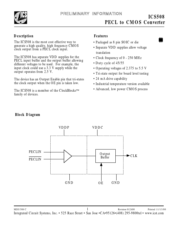
The ICS508 is the most cost effective way to generate a high quality, high frequency CMOS clock output from a PECL clock input. The ICS508 has separate VDD supplies for the PECL input buffer and the output buffer allowing different voltages to be used.
- Packaged as 8 pin SOIC or die
- Separate VDD supplies allow voltage translation
- Clock frequency of 0 - 250 MHz
- Duty cycle of 45/55
- Operating voltages of 2.375 to 5.5 V
- Tri-state output for board level testing
- 24 mA drive capability
- Industrial temperature version available
- Advanced, low power CMOS process