Datasheet4U Logo Datasheet4U.com

ICS7973I-147 - 1-TO-12 LVCMOS / LVTTL CLOCK MULTIPLIER/ZERO DELAY BUFFER

Description

The ICS87973I-147 is a LVCMOS/LVTTL clock generator and a member of the HiPerClockS™family of High Performance Clock Solutions from ICS.

The ICS87973I-147 has three selectable inputs and provides 14 LVCMOS/LVTTL outputs.

The ICS87973I-147 is a highly flexible device.

Features

  • Fully integrated PLL.
  • 14 LVCMOS/LVTTL outputs; (12) clock, (1) feedback, (1) sync.
  • Selectable LVCMOS/LVTTL or differential CLK, nCLK inputs.
  • CLK0, CLK1 can accept the following input levels: LVCMOS or LVTTL.
  • CLK, nCLK pair can accept the following differential input levels: LVPECL, LVDS, LVHSTL, SSTL, HCSL.
  • Output frequency range: 10MHz to 150MHz.
  • VCO range: 240MHz to 500MHz.
  • Output skew: 200ps (maximum).
  • Cycle-to-.

📥 Download Datasheet

Datasheet preview – ICS7973I-147

Datasheet Details

Part number ICS7973I-147
Manufacturer Integrated Circuit Systems
File Size 519.21 KB
Description 1-TO-12 LVCMOS / LVTTL CLOCK MULTIPLIER/ZERO DELAY BUFFER
Datasheet download datasheet ICS7973I-147 Datasheet
Additional preview pages of the ICS7973I-147 datasheet.
Other Datasheets by Integrated Circuit Systems

Full PDF Text Transcription

Click to expand full text
www.DataSheet4U.com Integrated Circuit Systems, Inc.
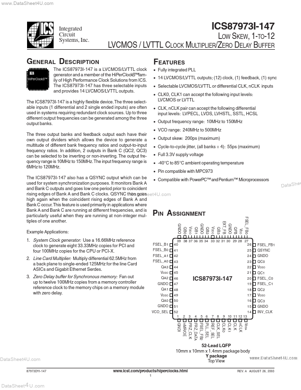
 ICS87973I-147 LOW SKEW, 1-TO-12 LVCMOS / LVTTL CLOCK MULTIPLIER/ZERO DELAY BUFFER FEATURES • Fully integrated PLL • 14 LVCMOS/LVTTL outputs; (12) clock, (1) feedback, (1) sync • Selectable LVCMOS/LVTTL or differential CLK, nCLK inputs • CLK0, CLK1 can accept the following input levels: LVCMOS or LVTTL • CLK, nCLK pair can accept the following differential input levels: LVPECL, LVDS, LVHSTL, SSTL, HCSL • Output frequency range: 10MHz to 150MHz • VCO range: 240MHz to 500MHz • Output skew: 200ps (maximum) • Cycle-to-cycle jitter, (all banks ÷ 4): 55ps (maximum) • Full 3.
Published: |