ICS8302I-01
ICS8302I-01 is 1-TO-2 LVCMOS / LVTTL FANOUT BUFFER W/ COMPLEMENTARY OUTPUT manufactured by Integrated Circuit Systems.
Integrated Circuit Systems, Inc.
LOW SKEW, 1-TO-2 LVCMOS / LVTTL FANOUT BUFFER W/ PLEMENTARY OUTPUT
Features
- plementary LVCMOS / LVTTL output
- LVCMOS / LVTTL clock input accepts LVCMOS or LVTTL input levels
- Maximum output frequency: 250MHz
- Output skew: 165ps (maximum)
- Part-to-part skew: 800ps (maximum)
- Small 8 lead SOIC package saves board space
- Full 3.3V or 3.3V core/2.5V output supply modes
- -40°C to 85°C ambient operating temperature
- Available in both standard and lead-free pliant packages
GENERAL DESCRIPTION
T h e I C S 8 3 0 2I-01 i s a l ow s kew, 1
- t o
- 2 LVCMOS/LVTTL Fanout Buffer w/plemen Hi Per Clock S™ tary Output a n d a m e m b e r o f t h e Hi Per Clock S ™family of High Performance Clock Solutions from ICS. The ICS8302I-01 has a single ended clock input. The single ended clock input accepts LVCMOS or LVTTL input levels. T h e ICS8302I-01 is characterized at full 3.3V for input VDD, and mixed 3.3V and 2.5V for output operating supply .. modes (VDDO). Guaranteed output and part-to-part skew characteristics make the ICS8302I-01 ideal for clock distribution applications demanding well defined performance and repeatability.
IC S
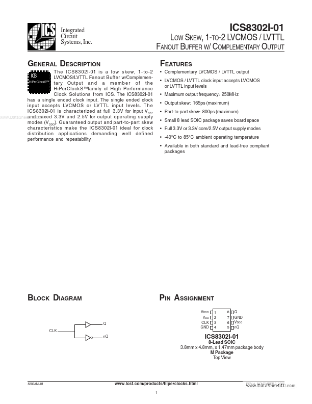
BLOCK DIAGRAM
Q CLK n Q
PIN ASSIGNMENT
VDDO VDD CLK GND 1 2 3 4 8 7 6 5 Q GND VDDO n Q
8-Lead SOIC 3.8mm x 4.8mm, x 1.47mm package body M Package Top View
8302AMI-01
.icst./products/hiperclocks.html
REV. A NOVEMBER 2, 2005
Integrated Circuit Systems, Inc.
LOW SKEW, 1-TO-2 LVCMOS / LVTTL FANOUT BUFFER W/ PLEMENTARY OUTPUT
Type Description Output supply pins. Power supply pin. Pulldown LVCMOS / LVTTL clock input. Power supply ground. plementary clock output. LVCMOS / LVTTL interface levels. Clock output. LVCMOS / LVTTL interface levels.
TABLE 1. PIN DESCRIPTIONS
Number 1, 6 2 3 4,7...