ICS8304-01
ICS8304-01 is 1-TO-4 LVCMOS / LVTTL INVERTING FANOUT BUFFER manufactured by Integrated Circuit Systems.
Integrated Circuit Systems, Inc.
LOW SKEW, 1-TO-4 LVCMOS / LVTTL INVERTING FANOUT BUFFER
Features
- 4 LVCMOS / LVTTL outputs
- LVCMOS/LVTTL clock input
- Maximum output frequency: 166MHz
- Output skew: 50ps (maximum)
- Part-to-part skew: 600ps (maximum)
- Small 8 lead SOIC package saves board space
- 3.3V input, outputs may be either 3.3V or 2.5V supply modes
- 0°C to 70°C ambient operating temperature
- Lead-Free package fully Ro HS pliant
GENERAL DESCRIPTION
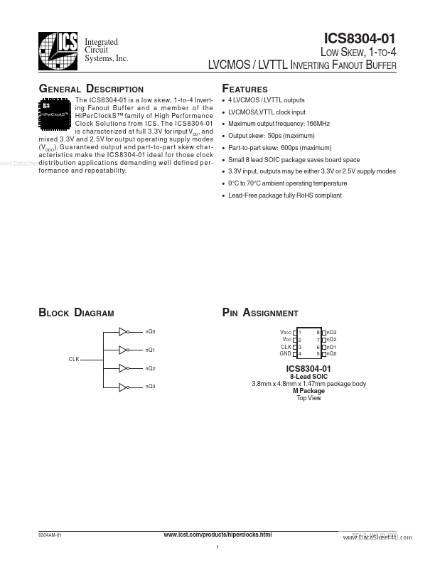
The ICS8304-01 is a low skew, 1-to-4 Inverting Fanout B u f fe r a n d a m e m b e r o f t h e Hi Per Clock S™ Hi Per Clock S ™ family of High Perfor mance Clock Solutions from ICS. The ICS8304-01 is characterized at full 3.3V for input VDD, and mixed 3.3V and 2.5V for output operating supply modes (VDDO). Guaranteed output and par t-to-par t skew characteristics make the ICS8304-01 ideal for those clock distribution applications demanding well defined per.. for mance and repeatability.
BLOCK DIAGRAM n Q0
PIN ASSIGNMENT
VDDO VDD CLK GND 1 2 3 4 8 7 6 5 n Q3 n Q2 n Q1 n Q0 n Q1 CLK n Q2
8-Lead SOIC 3.8mm x 4.8mm x 1.47mm package body M Package Top View n Q3
8304AM-01
.icst./products/hiperclocks.html
REV. D MAY 23, 2005
Integrated Circuit Systems, Inc.
LOW SKEW, 1-TO-4 LVCMOS / LVTTL INVERTING FANOUT BUFFER
Type Power Power Input Power Output Output Output Output Description Output supply pin. Core supply pin. Pulldown LVCMOS / LVTTL clock input. Power supply ground. Inver ted version of clock input. LVCMOS / LVTTL interface levels. Inver ted version of clock input. LVCMOS / LVTTL interface levels. Inver ted version of clock input. LVCMOS / LVTTL interface levels. Inver ted version of clock input. LVCMOS / LVTTL interface levels.
TABLE 1. PIN DESCRIPTIONS
Number 1 2 3 4 5
.. 6
Name VDDO VDD CLK GN D n Q0 n Q1 n Q2 n Q3
7 8
NOTE: Pulldown refers to internal input resistors. See Table 2, Pin Characteristics, for typical...