ICS83054I-01
ICS83054I-01 is SINGLE-ENDED MULTIPLEXER manufactured by Integrated Circuit Systems.
PRELIMINARY
Integrated Circuit Systems, Inc.
4-BIT, 2:1, SINGLE-ENDED MULTIPLEXER
GENERAL DESCRIPTION
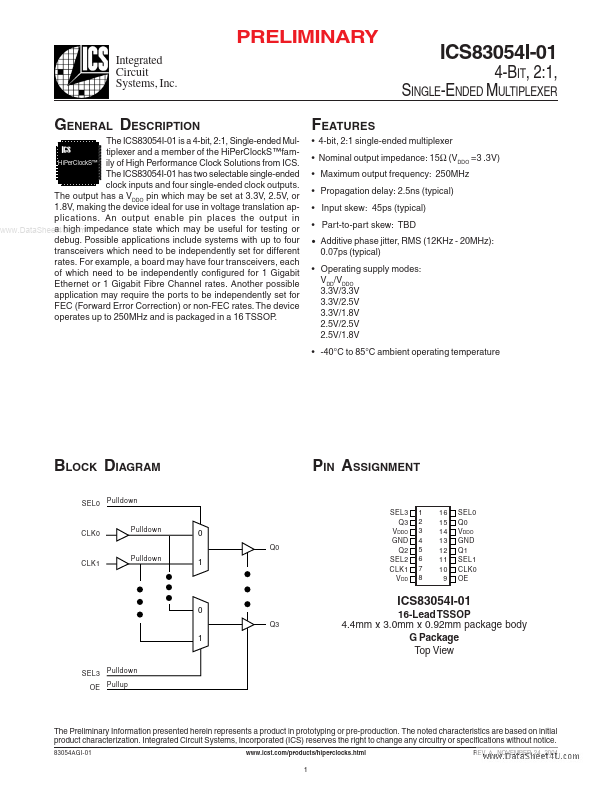
The ICS83054I-01 is a 4-bit, 2:1, Single-ended Multiplexer and a member of the Hi Per Clock S™fam Hi Per Clock S™ ily of High Performance Clock Solutions from ICS. The ICS83054I-01 has two selectable single-ended clock inputs and four single-ended clock outputs. The output has a VDDO pin which may be set at 3.3V, 2.5V, or 1.8V, making the device ideal for use in voltage translation applications. An output enable pin places the output in a high impedance state which may be useful for testing or .. debug. Possible applications include systems with up to four transceivers which need to be independently set for different rates. For example, a board may have four transceivers, each of which need to be independently configured for 1 Gigabit Ethernet or 1 Gigabit Fibre Channel rates. Another possible application may require the ports to be independently set for FEC (Forward Error Correction) or non-FEC rates. The device operates up to 250MHz and is packaged in a 16 TSSOP.
Features
- 4-bit, 2:1 single-ended multiplexer
- Nominal output impedance: 15Ω (VDDO =3 .3V)
- Maximum output frequency: 250MHz
- Propagation delay: 2.5ns (typical)
- Input skew: 45ps (typical)
- Part-to-part skew: TBD
- Additive phase jitter, RMS (12KHz
- 20MHz): 0.07ps (typical)
- Operating supply modes: VDD/VDDO 3.3V/3.3V 3.3V/2.5V 3.3V/1.8V 2.5V/2.5V 2.5V/1.8V
- -40°C to 85°C ambient operating temperature
BLOCK DIAGRAM
SEL0 Pulldown
PIN ASSIGNMENT
SEL3 Q3 VDDO GND Q2 SEL2 CLK1 VDD 1 2 3 4 5 6 7 8 16 15 14 13 12 11 10 9 SEL0 Q0 VDDO GND Q1 SEL1 CLK0 OE
CLK0
Pulldown
Q0
CLK1
Pulldown
Q3
16-Lead TSSOP 4.4mm x 3.0mm x 0.92mm package body G Package Top View
SEL3 Pulldown OE Pullup
The Preliminary Information presented herein represents a product in prototyping or pre-production. The noted characteristics are based on initial product...