ICS8344I
ICS8344I is 1-TO-24 DIFFERENTIAL-TO-LVCMOS FANOUT BUFFER manufactured by Integrated Circuit Systems.
Integrated Circuit Systems, Inc.
LOW SKEW, 1-TO-24 DIFFERENTIAL-TO-LVCMOS FANOUT BUFFER
Features
- 24 LVCMOS outputs, 7Ω typical output impedance
- 2 selectable differential clock input pairs for redundant clock applications
- CLKx, n CLKx pair can accept the following differential input levels: LVDS, LVPECL, LVHSTL, SSTL, HCSL
- Maximum output frequency up to 100MHz
- Translates any single-ended input signal to LVCMOS with resistor bias on n CLK input
- Multiple output enable pins for disabling unused outputs in reduced fanout applications
- Output skew: 275ps (maximum)
- Part-to-part skew: 600ps (maximum)
- Bank skew: 150ps (maximum)
- 3.3V, 2.5V or mixed 3.3V, 2.5V operating supply modes
- -40°C to 85°C ambient operating temperature
GENERAL DESCRIPTION
The ICS8344I is a low voltage, low skew fanout buffer and a member of the Hi Per Clock S™ Hi Per Clock S™ family of High Performance Clock Solutions from ICS. The ICS8344I has two selectable clock inputs. The CLK0, n CLK0 and CLK1, n CLK1 pairs can accept most standard differential input levels. The ICS8344I is designed to translate any differential signal levels to LVCMOS levels. The low impedance LVCMOS outputs are designed to drive 50Ω series or parallel terminated trans.. mission lines. The effective fanout can be increased to 48 by utilizing the ability of the outputs to drive two series terminated lines. Redundant clock applications can make use of the dual clock input. The dual clock inputs also facilitate board level testing. ICS8344I is characterized at full 3.3V, full 2.5V and mixed 3.3V input and 2.5V output operating supply modes.
,&6
Guaranteed output and part-to-part skew characteristics make the ICS8344I ideal for those clock distribution applications demanding well defined performance and repeatability.
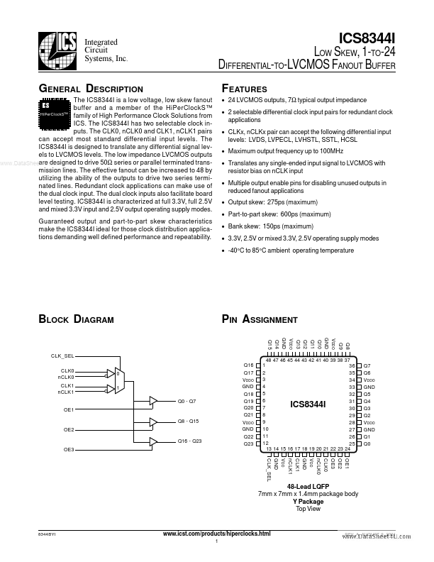
BLOCK DIAGRAM
PIN ASSIGNMENT
Q8 Q9 VDDO GND Q10 Q11 Q12 Q13 VDDO GND Q14 Q15
CLK_SEL CLK0 n CLK0 CLK1 n CLK1 Q16 Q17 VDDO GND Q18 Q19 Q20 Q21 VDDO GND Q22 Q23
0 1 Q0
- Q7
OE1...