ICS8745B
ICS8745B is 1:5 DIFFERENTIAL-TO-LVDS ZERO DELAY CLOCK GENERATOR manufactured by Integrated Circuit Systems.
Integrated Circuit Systems, Inc.
..
1:5 DIFFERENTIAL-TO-LVDS ZERO DELAY CLOCK GENERATOR
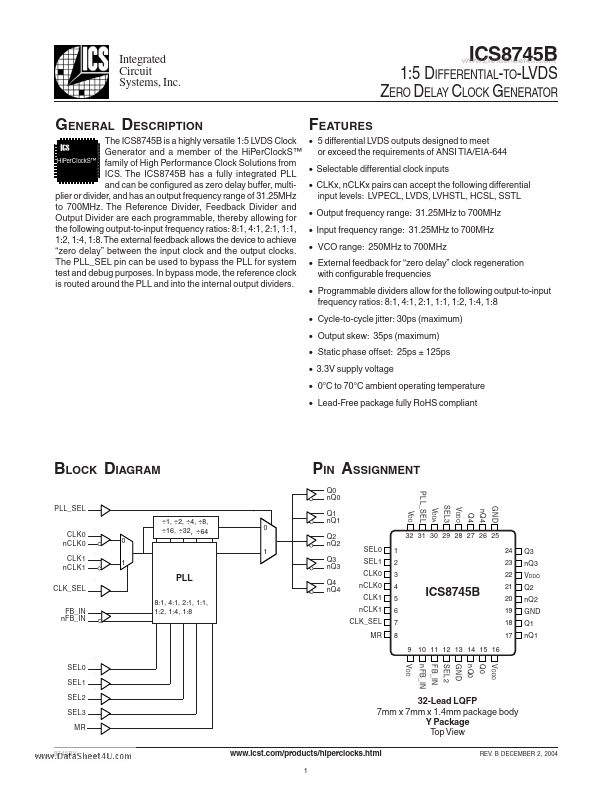
Features
- 5 differential LVDS outputs designed to meet or exceed the requirements of ANSI TIA/EIA-644
- Selectable differential clock inputs
- CLKx, nCLKx pairs can accept the following differential input levels: LVPECL, LVDS, LVHSTL, HCSL, SSTL
- Output frequency range: 31.25MHz to 700MHz
- Input frequency range: 31.25MHz to 700MHz
- VCO range: 250MHz to 700MHz
- External feedback for “zero delay” clock regeneration with configurable frequencies
- Programmable dividers allow for the following output-to-input frequency ratios: 8:1, 4:1, 2:1, 1:1, 1:2, 1:4, 1:8
-...