Datasheet4U Logo Datasheet4U.com

ICS9112-26 - Low Skew Output Buffer

General Description

a The ICS9112-26 a high performance, low skew, low jitter .D It is is clock driver.

designed to distribute high speed clocks in PC w systems operating at speeds from 0 to 133 MHz.

w wThe ICS9112-26 comes in an eight pin 150 mil SOIC package.

Key Features

  • Frequency range 0 - 133 MHz (3.3V) Less than 200 ps Jitter between outputs Skew controlled outputs Skew less than 250 ps between outputs Available in 8 pin 150 mil SOIC & 173 mil TSSOP packages. 3.3V ±10% operation Pin Configuration CLK1 CLK_IN CLK2 Pin.

📥 Download Datasheet

Datasheet Details

Part number ICS9112-26
Manufacturer Integrated Circuit Systems
File Size 103.12 KB
Description Low Skew Output Buffer
Datasheet download datasheet ICS9112-26 Datasheet

Full PDF Text Transcription (Reference)

The following content is an automatically extracted verbatim text from the original manufacturer datasheet and is provided for reference purposes only.

View original datasheet text
Integrated Circuit Systems, Inc. 
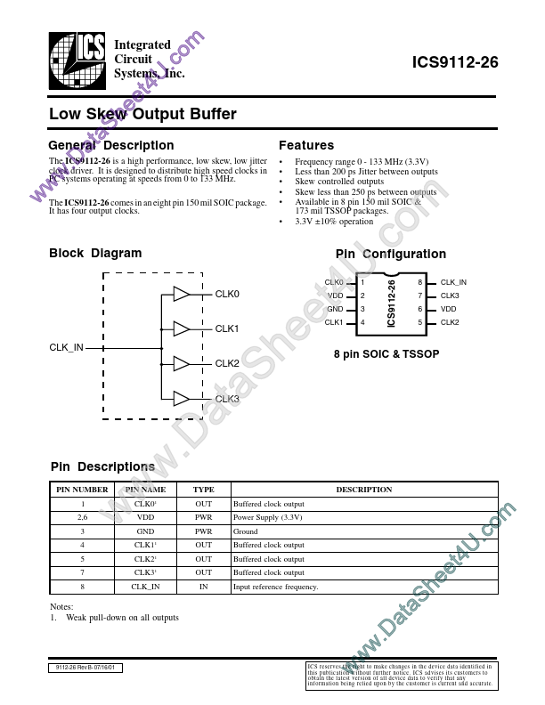
S a t General Description a The ICS9112-26 a high performance, low skew, low jitter .D It is is clock driver. designed to distribute high speed clocks in PC w systems operating at speeds from 0 to 133 MHz. w wThe ICS9112-26 comes in an eight pin 150 mil SOIC package. It has four output clocks. Block Diagram CLK0 Low Skew Output Buffer he 4 t e U . m o c ICS9112-26 Features • • • • • • Frequency range 0 - 133 MHz (3.3V) Less than 200 ps Jitter between outputs Skew controlled outputs Skew less than 250 ps between outputs Available in 8 pin 150 mil SOIC & 173 mil TSSOP packages. 3.3V ±10% operation Pin Configuration CLK1 CLK_IN CLK2 Pin Descriptions PIN NUMBER 1 2,6 3 4 5 7 8 PIN NAME w CLK0 VDD w 1 1 w .