ICS9148-46
ICS9148-46 is Pentium/ProTM System Clock Chip manufactured by Integrated Circuit Systems.
Integrated Circuit Systems, Inc.
Pentium/Pro TM System Clock Chip
General Description
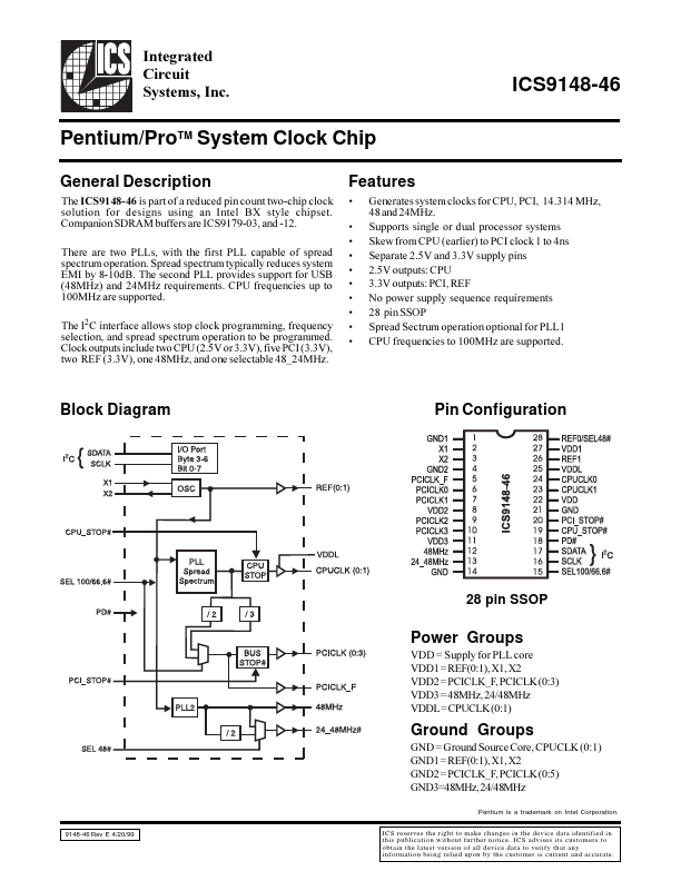
The ICS9148-46 is part of a reduced pin count two-chip clock solution for designs using an Intel BX style chipset. panion SDRAM buffers are ICS9179-03, and -12. There are two PLLs, with the first PLL capable of spread spectrum operation. Spread spectrum typically reduces system EMI by 8-10d B. The second PLL provides support for USB (48MHz) and 24MHz requirements. CPU frequencies up to 100MHz are supported. The I2C interface allows stop clock programming, frequency selection, and spread spectrum operation to be programmed. Clock outputs include two CPU (2.5V or 3.3V), five PCI (3.3V), two REF (3.3V), one 48MHz, and one selectable 48_24MHz.
Features
Generates system clocks for CPU, PCI, 14.314 MHz, 48 and 24MHz. Supports single or dual processor systems Skew from CPU (earlier) to PCI clock 1 to 4ns Separate 2.5V and 3.3V supply pins 2.5V outputs: CPU 3.3V outputs: PCI, REF No power supply sequence requirements 28 pin SSOP Spread Sectrum operation optional for PLL1 CPU frequencies to 100MHz are supported.
Block Diagram
Pin Configuration
28 pin SSOP
Power Groups
VDD = Supply for PLL core VDD1 = REF(0:1), X1, X2 VDD2 = PCICLK_F, PCICLK (0:3) VDD3 = 48MHz, 24/48MHz VDDL = CPUCLK (0:1)
Ground Groups
GND = Ground Source Core, CPUCLK (0:1) GND1 = REF(0:1), X1, X2 GND2 = PCICLK_F, PCICLK (0:5) GND3=48MHz, 24/48MHz
Pentium is a trademark on Intel Corporation. 9148-46 Rev E 4/20/99
ICS reserves the right to make changes in the device data identified in this publication without further notice. ICS advises its customers to obtain the latest version of all device data to verify that any information being relied upon by the customer is current and accurate.
Pin Descriptions
PIN NUMBER 1 2 3 4 5 6, 7, 9, 10 8 11 12 13 14 15 16 17 18 19 20 21 22 23, 24 25 26 27 28 PIN NAME GND1 X1 X2 GND2 PCICLK_F PCICLK (0:3) VDD2 VDD3 48MHz 24_48MHz GND3...