ICS9169C-272
ICS9169C-272 is Frequency Generator manufactured by Integrated Circuit Systems.
..
Integrated Circuit Systems, Inc.
Frequency Generator for Pentium™ Based Systems
General Description
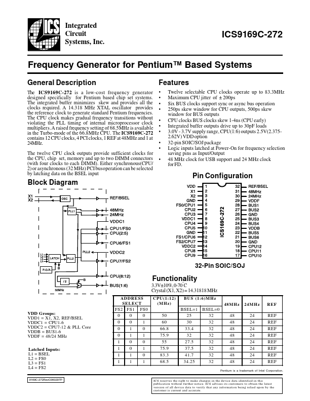
The ICS9169C-272 is a low-cost frequency generator designed specifically for Pentium based chip set systems. The integrated buffer minimizes skew and provides all the clocks required. A 14.318 MHz XTAL oscillator provides the reference clock to generate standard Pentium frequencies. The CPU clock makes gradual frequency transitions without violating the PLL timing of internal microprocessor clock multipliers. A raised frequency setting of 68.5MHz is available in the Turbo-mode of the 66.8MHz CPU. The ICS9169C-272 contains 12 CPU clocks, 4 PCI clocks, 1 REF at 48MHz and 1 at 24MHz. The twelve CPU clock outputs provide sufficient clocks for the CPU, chip set, memory and up to two DIMM connectors (with four clocks to each DIMM). Either synchronous(CPU/ 2) or asynchronous (32 MHz) PCI bus operation can be selected by latching data on the BSEL input
Features
- -
- -
- -
- -
- - Twelve selectable CPU clocks operate up to 83.3MHz Maximum CPU jitter of ± 200ps Six BUS clocks support sync or async bus operation 250ps skew window for CPU outputs, 500ps skew window for BUS outputs CPU clocks BUS clocks skew 1-4ns (CPU early) Integrated buffer outputs drive up to 30p F loads 3.0V
- 3.7V supply range, CPU(1:6) outputs 2.5V(2.3752.62V) VDD option 32-pin SOIC/SOJ package Logic inputs latched at Power-On for frequency selection saving pins as Input/Output 48 MHz clock for USB support and 24 MHz clock for FD.
Pin Configuration
Block Diagram
.
Data Shee
32-Pin SOIC/SOJ
3.3V±10%, 0-70°C Crystal (X1, X2) = 14.31818 MHz
A D D R E SS SELECT C PU (1:12) (M H z) BU S (1:6)M H z 48M H z 24M H z R EF
Functionality
VDD Groups: VDD1 = X1, X2, REF/BSEL VDDC1 = CPU1-6 VDDC2 = CPU7-12 & PLL Core VDDB = BUS1-6 VDDF = 48/24 MHz Latched Inputs: L1 = BSEL L2 = FS0 L3 = FS1 L4 = FS2 .
9169C-272Rev C060297P
FS2 FS1 0 0 0 0 0 1 0 1 1 0...