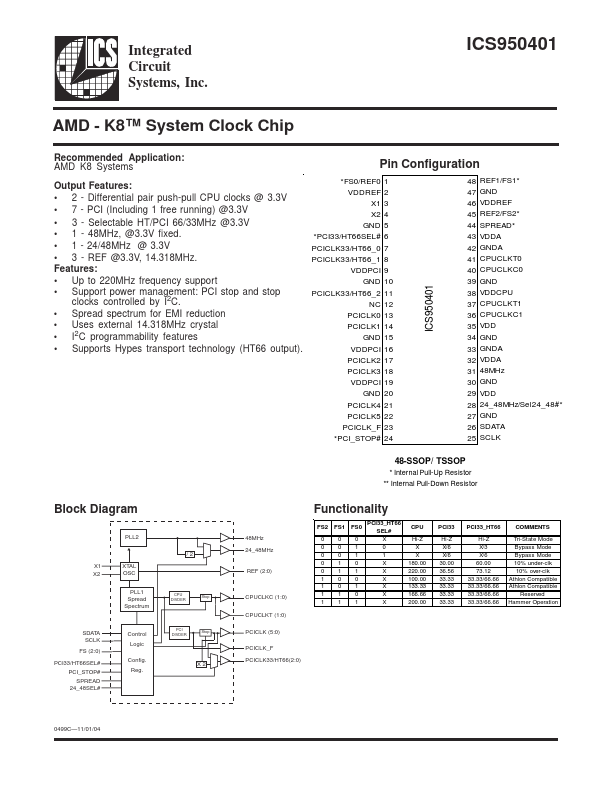
Datasheet4U Logo Datasheet4U.com

ICS950401 - System Clock

General Description

PIN # 1 2 3 4 5 6 7 8 9 10 11 12 13 14 15 16 17 18 19 20 21 22 23 24 25 26 27 28 29 30 31 32 33 34 35 36 37 38 39 40 41 42 43 44 45 46 47 48 PIN NAME FS0/REF0 VDDREF X1 X2 GND PCI33/HT66SEL# PCICLK33/HT66_0 PCICLK33/HT66_1 VDDPCI GND PCICLK33/HT66_2 NC PCICLK0 PCICLK1 GND VDDPCI PCICLK2 P

Key Features

  • VDDREF 2.
  • 2 - Differential pair push-pull CPU clocks @ 3.3V X1 3.
  • 7 - PCI (Including 1 free running) @3.3V X2 4.
  • 3 - Selectable HT/PCI 66/33MHz @3.3V GND 5.
  • 1 - 48MHz, @3.3V fixed.
  • PCI33/HT66SEL# 6.
  • 1 - 24/48MHz @ 3.3V PCICLK33/HT66_0 7.
  • 3 - REF @3.3V, 14.318MHz. PCICLK33/HT66_1 8 Features: VDDPCI 9.
  • Up to 220MHz frequency support GND 10.
  • Support power management: PCI stop and stop PCICLK33/HT66_2 11 clocks controlled.

📥 Download Datasheet

Datasheet Details

Part number ICS950401
Manufacturer Integrated Circuit Systems
File Size 108.63 KB
Description System Clock
Datasheet download datasheet ICS950401 Datasheet

Full PDF Text Transcription (Reference)

The following content is an automatically extracted verbatim text from the original manufacturer datasheet and is provided for reference purposes only.

View original datasheet text
Integrated Circuit Systems, Inc. ICS950401 AMD - K8™ System Clock Chip Recommended Application: AMD K8 Systems Pin Configuration *FS0/REF0 1 48 47 46 45 44 43 42 41 40 39 38 37 36 35 34 33 32 31 30 29 28 27 26 25 REF1/FS1* GND VDDREF REF2/FS2* SPREAD* VDDA GNDA CPUCLKT0 CPUCLKC0 GND VDDCPU CPUCLKT1 CPUCLKC1 VDD GND GNDA VDDA 48MHz GND VDD 24_48MHz/Sel24_48#* GND SDATA SCLK Output Features: VDDREF 2 • 2 - Differential pair push-pull CPU clocks @ 3.3V X1 3 • 7 - PCI (Including 1 free running) @3.3V X2 4 • 3 - Selectable HT/PCI 66/33MHz @3.3V GND 5 • 1 - 48MHz, @3.3V fixed. *PCI33/HT66SEL# 6 • 1 - 24/48MHz @ 3.3V PCICLK33/HT66_0 7 • 3 - REF @3.3V, 14.318MHz.