Datasheet4U Logo Datasheet4U.com

ICS950402 - System Clock

General Description

PIN # PIN NAME 1 FS0/REF0 2 VDDREF 3 X1 4 X2 5 GND 6 (PCICLK7/HTTCLK0)ModeA 7 PCICLK8/HTTCLK1/ModeB 8 PCICLK9/HTTCLK2 9 VDDPCI 10 GND 11 ~PCICLK10/HTTCLK3 12 PCICLK11 13 PCICLK0 14 PCICLK1 15 GND 16 VDDPCI 17 PCICLK2 18 PCICLK3 19 VDDPCI 20

Key Features

  • 2 - Differential pair push-pull CPU clocks @ 3.3V.
  • 9 - PCICLK (Including 1 free running) @3.3V.
  • FS0/REF0 1 VDDREF 2 X1 3 X2 4 GND 5 48 REF1/FS1.
  • 47 GND 46 VDDREF 45 REF2/FS2.
  • 44 Reset#.
  • 4 - Selectable PCICLK/HTTCLK @3.3V.
  • 1 - 48MHz, @3.3V fixed.
  • 1 - 24/48MHz @ 3.3V.
  • 3 - REF @3.3V, 14.318MHz. Features:.
  • Programmable output frequency.
  • (PCICLK7/HTTCLK0)ModeA 6.
  • PCICLK8/HTTCLK1/ModeB 7 PCICLK9/HTTCLK2 8 VDDPCI.

📥 Download Datasheet

Datasheet Details

Part number ICS950402
Manufacturer Integrated Circuit Systems
File Size 180.37 KB
Description System Clock
Datasheet download datasheet ICS950402 Datasheet

Full PDF Text Transcription (Reference)

The following content is an automatically extracted verbatim text from the original manufacturer datasheet and is provided for reference purposes only.

View original datasheet text
Integrated Circuit Systems, Inc. ICS950402 AMD - K8™ System Clock Chip Recommended Application: AMD K8 System Clock with AMD or VIA Chipset
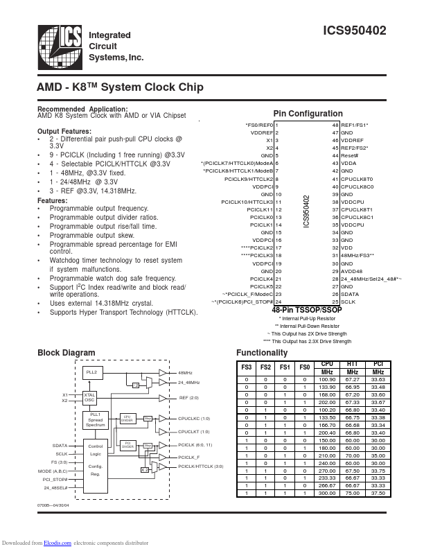
 Pin Configuration Output Features: • 2 - Differential pair push-pull CPU clocks @ 3.3V • 9 - PCICLK (Including 1 free running) @3.3V *FS0/REF0 1 VDDREF 2 X1 3 X2 4 GND 5 48 REF1/FS1* 47 GND 46 VDDREF 45 REF2/FS2* 44 Reset# • 4 - Selectable PCICLK/HTTCLK @3.3V • 1 - 48MHz, @3.3V fixed. • 1 - 24/48MHz @ 3.3V • 3 - REF @3.3V, 14.318MHz. Features: • Programmable output frequency. *(PCICLK7/HTTCLK0)ModeA 6 *PCICLK8/HTTCLK1/ModeB 7 PCICLK9/HTTCLK2 8 VDDPCI 9 GND 10 PCICLK10/HTTCLK3 11 PCICLK11 12 43 VDDA 42 GND 41 CPUCLK8T0 40 CPUCLK8C0 39 GND 38 VDDCPU 37 CPUCLK8T1 ICS950402 • Programmable output divider ratios.