Datasheet4U Logo Datasheet4U.com

ICS954119 - Programmable Timing Control Hub

Description

PIN # PIN NAME 1 2 3 4 5 6 7 8 GND PCICLK3 PCICLK4 PCICLK5 GND VDDPCI PCICLK_F0 FSLA/PCICLK_F1 PIN TYPE PWR OUT OUT OUT PWR PWR OUT I/O DESCRIPTION Ground pin.

PCI clock output.

PCI clock output.

Features

  • 2 - 0.7V current-mode differential CPU pairs.
  • 1 - 0.7V current-mode differential SRC pair.
  • 6 - PCI (33MHz).
  • 3 - PCICLK_F, (33MHz) free-running.
  • 1 - USB, 48MHz.
  • 1 - 24/48 MHz.
  • 1 - DOT, 96MHz, 0.7V current differential pair.
  • 2 - REF, 14.318MHz.
  • 5 - PCI-Express 0.7V current differential pairs Key Specifications:.
  • CPU/SRC outputs cycle-cycle jitter < 85ps.
  • PCI outputs cycle-cycle jitter < 250ps.

📥 Download Datasheet

Datasheet preview – ICS954119

Datasheet Details

Part number ICS954119
Manufacturer Integrated Circuit Systems
File Size 395.15 KB
Description Programmable Timing Control Hub
Datasheet download datasheet ICS954119 Datasheet
Additional preview pages of the ICS954119 datasheet.
Other Datasheets by Integrated Circuit Systems

Full PDF Text Transcription

Click to expand full text
www.DataSheet4U.com Integrated Circuit Systems, Inc. ICS954119 Advance Information Programmable Timing Control Hub™ for Next Gen P4™ processor Recommended Application: CK410 compliant clock Output Features: • 2 - 0.7V current-mode differential CPU pairs • 1 - 0.7V current-mode differential SRC pair • 6 - PCI (33MHz) • 3 - PCICLK_F, (33MHz) free-running • 1 - USB, 48MHz • 1 - 24/48 MHz • 1 - DOT, 96MHz, 0.7V current differential pair • 2 - REF, 14.318MHz • 5 - PCI-Express 0.7V current differential pairs Key Specifications: • CPU/SRC outputs cycle-cycle jitter < 85ps • PCI outputs cycle-cycle jitter < 250ps • 
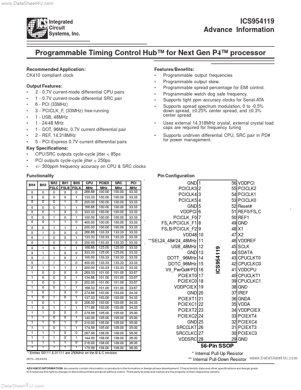
+/- 300ppm frequency accuracy on CPU & SRC clocks Functionality Bit2 Bit1 Bit0 CPU PCIEX SRC Bit4 Bit3 FSLC FSLB FSLA MHz MHz MHz 266.66 100.00 100.00 0 0 0 0 0 133.33 100.00 100.
Published: |