DESCRIPTION
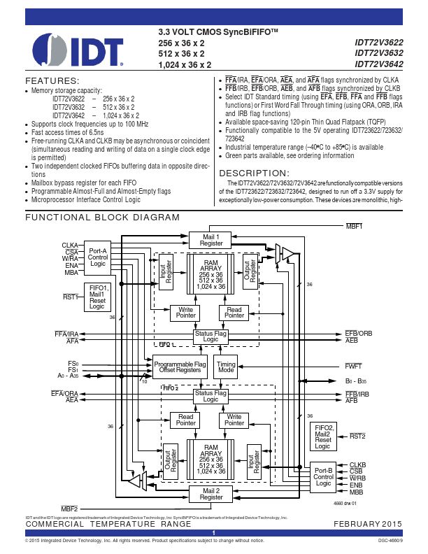
: Two independent 256/512/1,024 x 36 dual-port SRAM FIFOs on board each chip buffer data in opposite directions. Communication between .UNCTIONAL BLOCK DIAGRAM CLKA CSA W/RA ENA MBA Mail 1 Register Input Register RAM ARRAY 256 x 36 512 x 36 1,024 x 36 Output Register Port-A Control Logic MBF1 RST1 FIFO1, Mail1 Reset Logic 36 36 Write Pointer Read Pointer EFB/ORB AEB FFA/IRA AFA FIFO 1 Status Flag Logic FS0 FS1 A0 - A35 10 Programmable Flag Offset Registers FIFO 2 Timing Mode FWFT B0 - B35 EFA/ORA AEA Status Flag Logic Write Pointer 36 FFB/IRB AFB 36 Read Pointer RAM ARRAY 256 x 36 512 x 36 1,024 x 36 Mail 2 Register Output Register FIFO2, Mail2 Reset Logic Input Register RST2 Port-B Control Logic CLKB CSB W/RB ENB MBB 4660 drw 01 MBF2 IDT, the IDT logo are registered trademarks of Integrated Device Technology, Inc. SyncBiFIFO is a trademark of Integrated Device Technology, Inc. COMMERCIAL TEMPERATURE RANGE DECEMBER 2001 DSC-4660/4 1 2001 Integrated Device Technology, Inc. All rights reserved. Integrated Device Tech