IDT72V71643
IDT72V71643 is 3.3 VOLT TIME SLOT INTERCHANGE DIGITAL SWITCH manufactured by Integrated Device Tech.
3.3 VOLT TIME SLOT INTERCHANGE DIGITAL SWITCH WITH RATE MATCHING 4,096 x 4,096
Features
:
- -
- -
- -
- -
- -
- -
- -
- IDT72V71643
Up to 32 serial input and output streams Maximum 4,096 x 4,096 channel non-blocking switching Accepts data streams at 2.048 Mb/s, 4.096 Mb/s, 8.192 Mb/s or 16.384 Mb/s Rate matching capability: Mux/Demux mode and Split mode Output Enable Indication Pins Per-channel Variable Delay mode for low-latency applications Per-channel Constant Delay mode for frame integrity applications Automatic identification of ST-BUS® and GCI serial streams Automatic frame offset delay measurement Per-stream frame delay offset programming Per-channel high-impedance output control Per-channel Processor mode to allow microprocessor writes to TX streams Direct microprocessor access to all internal memories Memory block programming for quick setup IEEE-1149.1 (JTAG) Test Port
- -
- -
Internal Loopback for testing Available in 144-pin Thin Quad Flatpack (TQFP) and 144-pin Ball Grid Array (BGA) packages Operating Temperature Range -40°C to +85°C 3.3V I/O with 5V tolerant inputs and TTL patible outputs
DESCRIPTION:
The IDT72V71643 has a maximum non-blocking switch capacity of 4,096 x 4,096 channels with data rates at 2.048 Mb/s, 4.096 Mb/s, 8.192 Mb/s or 16.384 Mb/s. With 32 inputs and 32 outputs, a variety of rate binations is supported, under either Mux/Demux mode or Split mode, to allow for switching between streams of different data rates. Output enable indications are provided through optional pins (one pin per output stream, only 16 output streams can be used in this mode) to facilitate external data bus control. For applications requiring 32 streams and 32 per-stream Output Enable indicators, there is also an All Output Enable Feature.
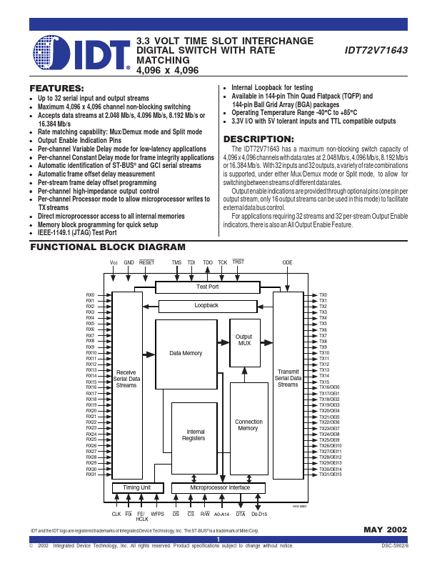
FUNCTIONAL BLOCK DIAGRAM
Vcc GND RESET TMS TDI TDO TCK TRST ODE
Test Port
RX0 RX1 RX2 RX3 RX4 RX5 RX6 RX7 RX8 RX9 RX10 RX11 RX12 RX13 RX14 RX15 RX16 RX17 RX18 RX19 RX20 RX21 RX22 RX23 RX24 RX25 RX26 RX27 RX28 RX29...