IDT72V851
IDT72V851 is CMOS FIFO manufactured by Integrated Device Tech.
3.3 VOLT DUAL CMOS Sync FIFO™ DUAL 256 X 9, DUAL 512 X 9, DUAL 1,024 X 9, DUAL 2,048 X 9, DUAL 4,096 X 9 , DUAL 8,192 X 9
IDT72V801 IDT72V811 IDT72V821 IDT72V831 IDT72V841 IDT72V851
.EATURES:
- -
- -
- -
- -
- -
- -
- -
- The IDT72V801 is equivalent to two IDT72V201 256 x 9 FIFOs The IDT72V811 is equivalent to two IDT72V211 512 x 9 FIFOs The IDT72V821 is equivalent to two IDT72V221 1,024 x 9 FIFOs The IDT72V831 is equivalent to two IDT72V231 2,048 x 9 FIFOs The IDT72V841 is equivalent to two IDT72V241 4,096 x 9 FIFOs The IDT72V851 is equivalent to two IDT72V251 8,192 x 9 FIFOs Offers optimal bination of large capacity, high speed, design flexibility and small footprint Ideal for prioritization, bidirectional, and width expansion applications 10 ns read/write cycle time 5V input tolerant Separate control lines and data lines for each FIFO Separate Empty, Full, programmable Almost-Empty and Almost-Full flags for each FIFO Enable puts output data lines in high-impedance state Space-saving 64-pin plastic Thin Quad Flat Pack (TQFP/ STQFP) Industrial temperature range (- 40°C to +85°C) is available
DESCRIPTION:
The IDT72V801/72V811/72V821/72V831/72V841/72V851/72V851 are dual synchronous (clocked) FIFOs. The device is functionally equivalent to two IDT72V201/72V211/72V221/72V231/72V241/72V251 FIFOs in a single package with all associated control, data, and flag lines assigned to separate pins.
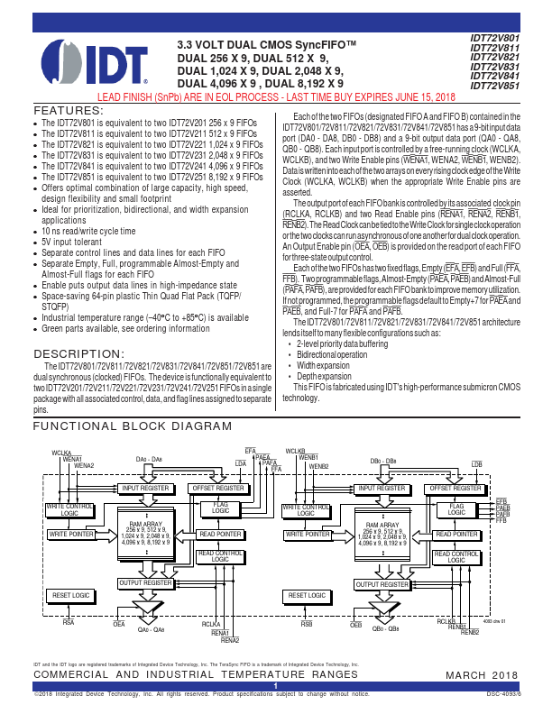
Each of the two FIFOs (designated FIFO A and FIFO B) contained in the IDT72V801/72V811/72V821/72V831/72V841/72V851 has a 9-bit input data port (DA0
- DA8, DB0
- DB8) and a 9-bit output data port (QA0
- QA8, QB0
- QB8). Each input port is controlled by a free-running clock (WCLKA, WCLKB), and two Write Enable pins (WENA1, WENA2, WENB1, WENB2). Data is written into each of the two arrays on every rising clock edge of the Write Clock (WCLKA, WCLKB) when the appropriate Write Enable pins are asserted. The output port of each FIFO bank is controlled by its associated clock pin...