Integrated Device Tech IDT74FCT3574A
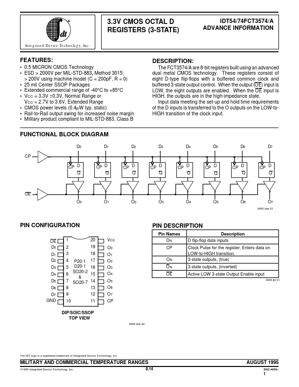
The FCT3574/A are 8-bit registers built using an advanced dual metal CMOS technology. These registers consist of eight D-type flip-flops with a buffered common clock and buffered 3-state output control.| Part No. | IDT74FCT3574A |
|---|---|
| Datasheet | IDT74FCT3574A Download |
| Manufacturer |  Integrated Device Tech |
| Description | 3.3V CMOS OCTAL D REGISTERS (3-STATE) |
| Buy | Stock & Price |
FEATURES
:● 0.5 MICRON CMOS Technology
● ESD > 2000V per MIL-STD-883, Method 3015; > 200V using machine model (C = 200pF, R = 0)
● 25 mil Center SSOP Packages
● Extended commercial range of -40°C to +85°C
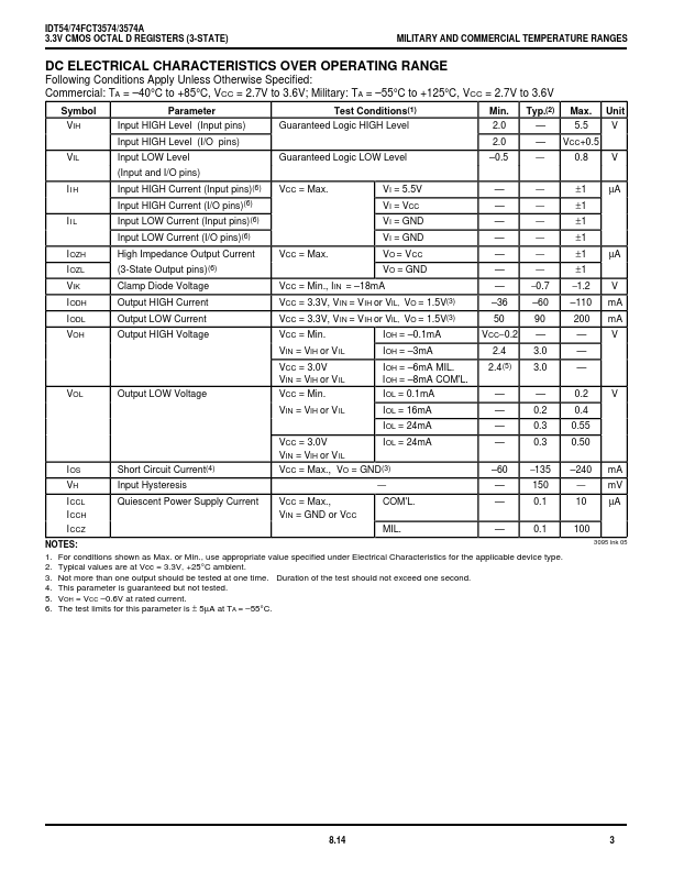
● VCC = 3.3V ± 0.3V, Normal Range or VCC = 2.7V to 3.6V, Extended Range
● CMOS power levels (0.4µW typ. static)
● Rail-to-Rail output swing for increased noise margin
● Military product compliant to MIL-STD-883, Class B
DESCRIPTION
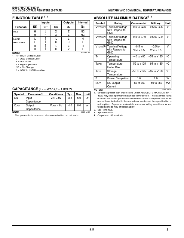
: When the output (OE) input is LOW, the eight outputs are enabled. When the OE input is HIGH, the outputs are in the high-impedance state. Input data meeting the set-up and hold time requirements of the D inputs is transferred to the O outputs on the LOW-toHIGH transition of the clock input. FUNCTIONAL BLOCK DIAGRAM D0 CP CP D Q CP D Q CP D Q CP D Q CP D Q CP D Q CP D Q CP D Q D1 D2 D3 D4 D5 D6 D7 OE O0 O1 O2 O3 O4 O5 O6 O7 3095 drw 01 PIN CONFIGURATION OE D0 D1 D2 D3 D4 D5 D6 D7 GND 1 2 3 4 P20-1 5 D20-1 SO20-2 6 & 7 SO20-7 8 9 10 20 19 18 17 16 15 14 13 12 11 VCC O0 O1 O2 O3 O4 O5 O6 O7 CP PINDESCRIPTION
Pin Names DN CP ONDESCRIPTION
D flip-flop data inputs Clock Pulse for the register.