ICS9LP525-2
ICS9LP525-2 is 56-pin CK505 Clock manufactured by Integrated Device Technology.
..net
56-pin CK505 for Intel Desktop Systems
Remended Application: CK505 clock, 56-pin Intel Yellow Cover part Output Features
:
- 2
- CPU differential low power push-pull pairs
- 7- SRC differential low power push-pull pairs
- 1
- CPU/SRC selectable differential low power push-pull pair
- 1
- SRC/DOT selectable differential low power push-pull pair
- 5
- PCI, 33MHz
- 1
- PCI_F, 33MHz free running
- 1
- USB, 48MHz
- 1
- REF, 14.318MHz Key Specifications:
- CPU outputs cycle-cycle jitter < 85ps
- SRC output cycle-cycle jitter < 125ps
- PCI outputs cycle-cycle jitter < 250ps
- +/- 100ppm frequency accuracy on all outputs
- SRC are PCIe Gen2 pliant
Features
/Benefits:
- Supports spread spectrum modulation, default is 0.5% down spread
- Uses external 14.318MHz crystal, external crystal load caps are required for frequency tuning
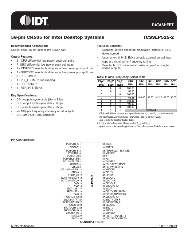
- Selectable SRC differential push-pull pair/two single ended outputs Table 1: CPU Frequency Select Table
FSLC B0b7 0 0 0 0 1 1 1...