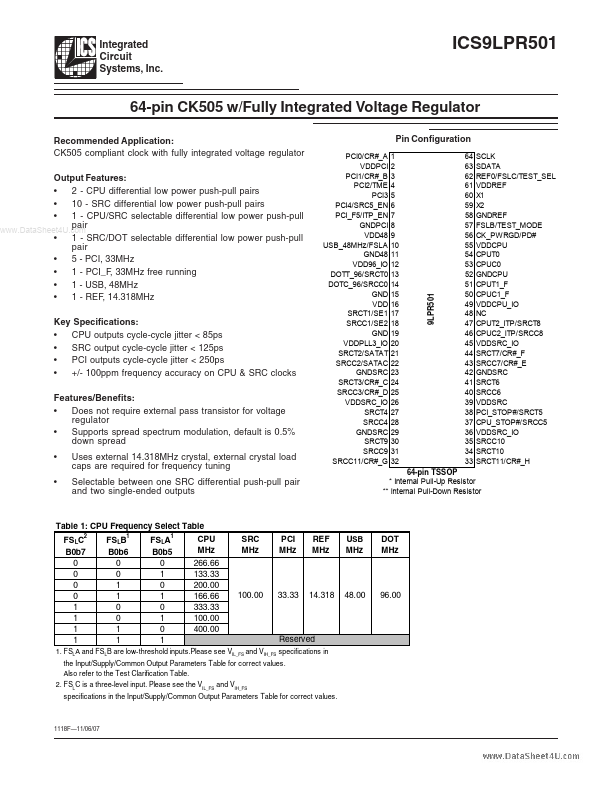
ICS9LPR501
ICS9LPR501 is 64-pin CK505 w/Fully Integrated Voltage Regulator manufactured by Integrated Device Technology.
Integrated Circuit Systems, Inc.
64-pin CK505 w/Fully Integrated Voltage Regulator
Remended Application: CK505 pliant clock with fully integrated voltage regulator Output Features
:
- 2
- CPU differential low power push-pull pairs
- 10
- SRC differential low power push-pull pairs
- 1
- CPU/SRC selectable differential low power push-pull pair ..
- 1
- SRC/DOT selectable differential low power push-pull pair
- 5
- PCI, 33MHz
- 1
- PCI_F, 33MHz free running
- 1
- USB, 48MHz
- 1
- REF, 14.318MHz Key Specifications:
- CPU outputs cycle-cycle jitter < 85ps
- SRC output cycle-cycle jitter < 125ps
- PCI outputs cycle-cycle jitter < 250ps
- +/- 100ppm frequency...