IDT5P49V5901
IDT5P49V5901 is Programmable Clock Generator manufactured by Integrated Device Technology.
Programmable Clock Generator
PRELIMINARY DATASHEET
Description
The IDT5P49V5901 is a programmable clock generator intended for high performance consumer, networking, industrial, puting, and data-munications applications. Configurations may be stored in on-chip One-Time Programmable (OTP) memory or changed using I2C interface. This is IDTs fifth generation of programmable clock technology (Versa Clock® 5). The frequencies are generated from a single reference clock. The reference clock can e from one of the two redundant clock inputs. A glitchless manual switchover function allows one of the redundant clocks to be selected during normal operation. Two select pins allow up to 4 different configurations to be programmed and accessible using processor GPIOs or bootstrapping. The different selections may be used for different operating modes (full function, partial function, partial power-down), regional standards (US, Japan, Europe) or system production margin testing. The device may be configured to use one of two I2C addresses to allow multiple devices to be used in a system.
Features
- Generates up to four independent output frequencies
- High performance, low phase noise PLL, <0.7 ps RMS typical phase jitter on outputs:
- PCIe Gen1, 2, 3 pliant clock capability
- USB 3.0 pliant clock capability
- 1 Gb E and 10 Gb E
- Four fractional output dividers (FODs)
- Independent Spread Spectrum capability on each output pair
- Four banks of internal non-volatile in-system programmable or factory programmable OTP memory
- I2C serial programming interface
- One reference LVCMOS output clock
- Four universal output pairs:
- Each configurable as one differential output pair or two LVCMOS outputs I/O Standards:
- Single-ended I/Os: 1.8V to 3.3V LVCMOS
- Differential I/Os
- LVPECL, LVDS and HCSL
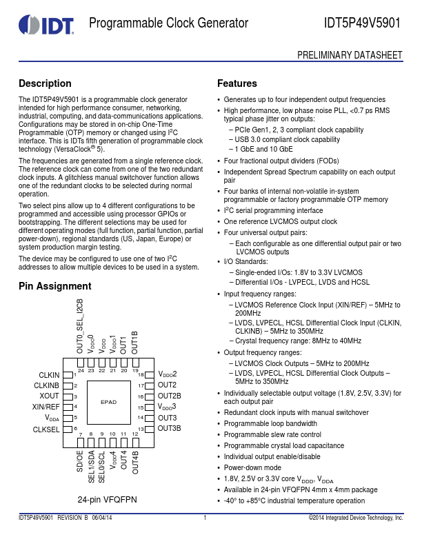
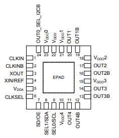
- Pin Assignment
OUT0_SEL_I2CB
- Input frequency ranges:
- LVCMOS Reference Clock Input (XIN/REF)
- 5MHz to 200MHz
- LVDS, LVPECL, HCSL Differential...
Representative IDT5P49V5901 image (package may vary by manufacturer)