IDT70V3319 Overview
Key Features
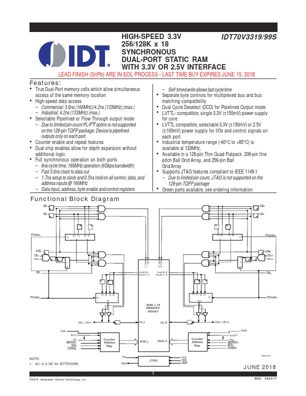
- I/O17L Din_L Din_R I/O0R
| Part | IDT70V3319 |
|---|---|
| Description | SYNCHRONOUS DUAL-PORT STATIC RAM |
| Manufacturer | Integrated Device Technology |
| Size | 309.20 KB |
| Part Number | Manufacturer | Description |
|---|---|---|
| IDT70V3319S | IDT | SYNCHRONOUS DUAL-PORT STATIC RAM |