IDT72T40118
Key Features
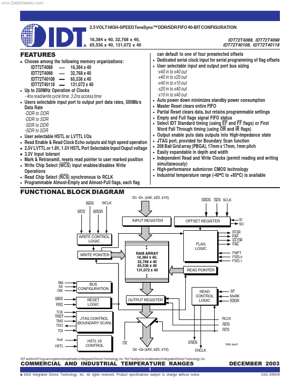
- Choose among the following memory organizations: IDT72T4088 16,384 x 40 IDT72T4098 32,768 x 40 IDT72T40108 65,536 x 40 IDT72T40118 131,072 x 40 Up to 250MHz Operation of Clocks - 4ns read/write cycle time, 3.2ns access time Users selectable input port to output port data rates, 500Mb/s Data Rate -DDR to DDR -DDR to SDR -SDR to DDR -SDR to SDR User selectable HSTL or LVTTL I/Os Read Enable & Read Clock Echo outputs aid high speed operation 2.5V LVTTL or 1.8V, 1.5V HSTL Port Selectable Input/Ouput voltage 3.3V Input tolerant Mark & Retransmit, resets read pointer to user marked position Write Chip Select (WCS) input enables/disables Write Operations Read Chip Select (RCS) synchronous to RCLK Programmable Almost-Empty and Almost-Full flags, each flag * * * * * * * * * * *
- can default to one of four preselected offsets Dedicated serial clock input for serial programming of flag offsets User selectable input and output port bus sizing -x40 in to x40 out -x40 in to x20 out -x40 in to x10 out -x20 in to x40 out -x10 in to x40 out Auto power down minimizes standby power consumption Master Reset clears entire FIFO Partial Reset clears data, but retains programmable settings Empty and Full flags signal FIFO status Select IDT Standard timing (using EF and FF flags) or First Word Fall Through timing (using OR and IR flags) Output enable puts data outputs into High-Impedance state JTAG port, provided for Boundary Scan function 208 Ball Grid array (PBGA), 17mm x 17mm, 1mm pitch Easily expandable in depth and width Independent Read and Write Clocks (permit reading and writing simultaneously) High-performance submicron CMOS technology Industrial temperature range (-40°C to +85°C) is avail