IDT8T79S818I-08
Overview
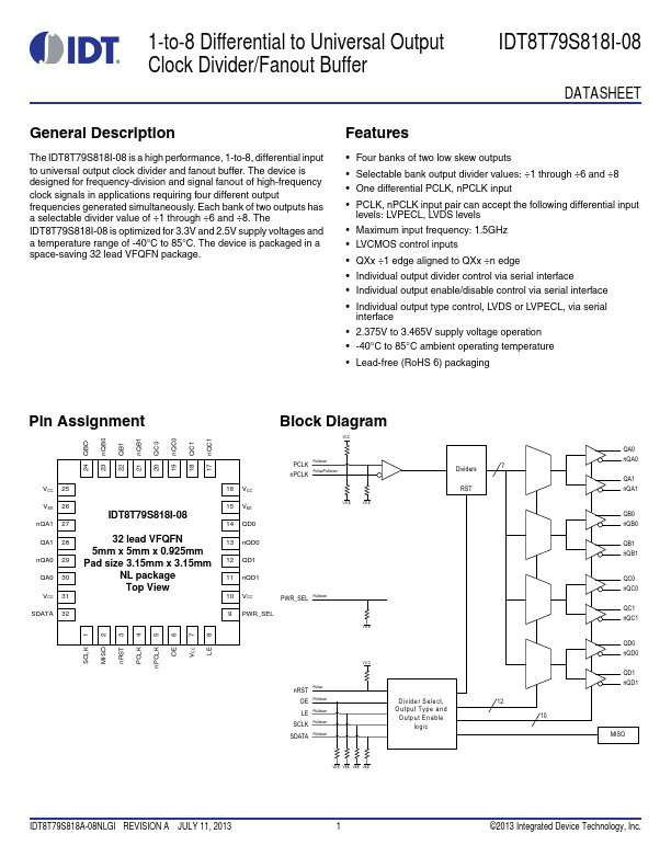
The IDT8T79S818I-08 is a high performance, 1-to-8, differential input to universal output clock divider and fanout buffer. The device is designed for frequency-division and signal fanout of high-frequency clock signals in applications requiring four different output frequencies generated simultaneously.
- Four banks of two low skew outputs
- Selectable bank output divider values: ÷1 through ÷6 and ÷8
- One differential PCLK, nPCLK input
- PCLK, nPCLK input pair can accept the following differential input levels: LVPECL, LVDS levels
- Maximum input frequency: 1.5GHz
- LVCMOS control inputs *