IDTCV119E
Overview
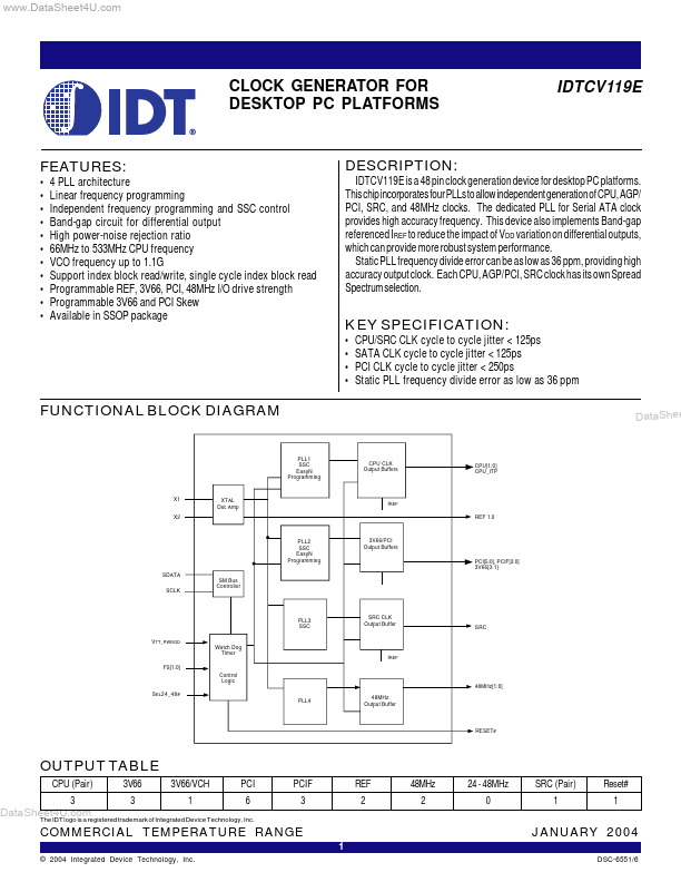
KEY SPECIFICATION: * * CPU/SRC CLK cycle to cycle jitter < 125ps SATA CLK cycle to cycle jitter < 125ps PCI CLK cycle to cycle jitter < 250ps Static PLL frequency divide error as low as 36 ppm FUNCTIONAL BLOCK DIAGRAM PLL1 SSC EasyN Programming CPU CLK Output Buffers CPU[1:0] CPU_ITP DataShee X1 XTAL Osc Amp IREF REF 1.0 X2 PLL2 SSC EasyN Programming SDATA SCLK SM Bus Controller 3V66/PCI Output Buffers PCI[5:0], PCIF[2:0] 3V66[3:1] PLL3 SSC VTT_PWRGD Watch Dog Timer FS[1:0] Control Logic SRC CLK Output Buffer SRC IREF 48MHz[1:0] S EL24_48# PLL4 48MHz Output Buffer RESET# OUTPUT.
- 4 PLL architecture Linear frequency programming Independent frequency programming and SSC control Band-gap circuit for differential output High power-noise rejection ratio 66MHz to 533MHz CPU frequency VCO frequency up to 1.1G Support index block read/write, single cycle index block read Programmable REF, 3V66, PCI, 48MHz I/O drive strength Programmable 3V66 and PCI Skew Available in SSOP package