IDT74LVC244A
IDT74LVC244A is 3.3V CMOS OCTAL BUFFER/DRIVER WITH 3-STATE OUTPUTS/ 5 VOLT TOLERANT I/O manufactured by Integrated Device.
IDT74LVC244A 3.3V CMOS OCTAL BUFFER/DRIVER WITH 3-STATE OUTPUTS
INDUSTRIAL TEMPERATURE RANGE
3.3V CMOS OCTAL BUFFER/DRIVER WITH 3-STATE OUTPUTS, 5 VOLT TOLERANT I/O
- 0.5 MICRON CMOS Technology
- ESD > 2000V per MIL-STD-883, Method 3015; > 200V using machine model (C = 200p F, R = 0)
- VCC = 3.3V ± 0.3V, Normal Range
- VCC = 2.7V to 3.6V, Extended Range
- CMOS power levels (0.4µ W typ. static)
- Rail-to-rail output swing for increased noise margin
- All inputs, outputs, and I/O are 5V tolerant
- Supports hot insertion
- Available in SOIC, SSOP, QSOP, and TSSOP packages
Features
:
DESCRIPTION:
DRIVE Features
: APPLICATIONS:
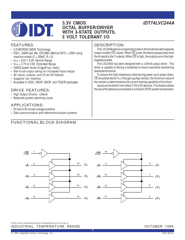
The LVC244A device is organized as two 4-bit line drivers with separate output-enable (OE) inputs. When OE is low, the device passes data from the A inputs to the Y outputs. When OE is high, the outputs are in the highimpedance state. The LVC244A has been designed with a ±24m A output driver. This driver is capable of driving a moderate to heavy load while maintaining speed performance. To ensure the high-impedance state during power up or power down, OE should be tied to VCC through a pullup resistor; the minimum value of the resistor is determined by the current-sinking capability of the driver. Inputs can be driven from either 3.3V or 5V devices. This feature allows the use of this device as a translator in a mixed 3.3V/5V system environment.
- High Output Drivers: ±24m A
- Reduced system switching noise
- 5V and 3.3V mixed voltage systems
- Data munication and telemunication systems
FUNCTIONAL BLOCK DIAGRAM
1OE
2OE
1A1
1Y1
2A1
2Y1
1A2...