IDTQS3244
IDTQS3244 is HIGH-SPEED CMOS QUICKSWITCH 8-BIT BUS SWITCH manufactured by Integrated Device.
IDTQS3244 HIGH-SPEED CMOS QUICKSWITCH 8-BIT BUS SWITCH
INDUSTRIAL TEMPERATURE RANGE
QUICKSWITCH® PRODUCTS HIGH-SPEED CMOS QUICKSWITCH 8-BIT BUS SWITCH
- -
- -
- -
Features
:
Enhanced N channel FET with no inherent diode to Vcc 25Ω bidirectional switches connect inputs to outputs Pin patible with 74F244, 74FCT244, and 74FCT244T Zero propagation delay, zero ground bounce Undershoot clamp diodes on all switch and control inputs Available in QSOP, SOIC, and TSSOP packages
APPLICATIONS:
- -
- -
- -
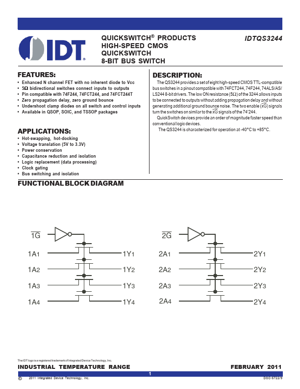
- The QS3244 provides a set of eight high-speed CMOS TTL-patible bus switches in a pinout patible with 74FCT244, 74F244, 74ALS/AS/ LS244 8-bit drivers. The low ON resistance...