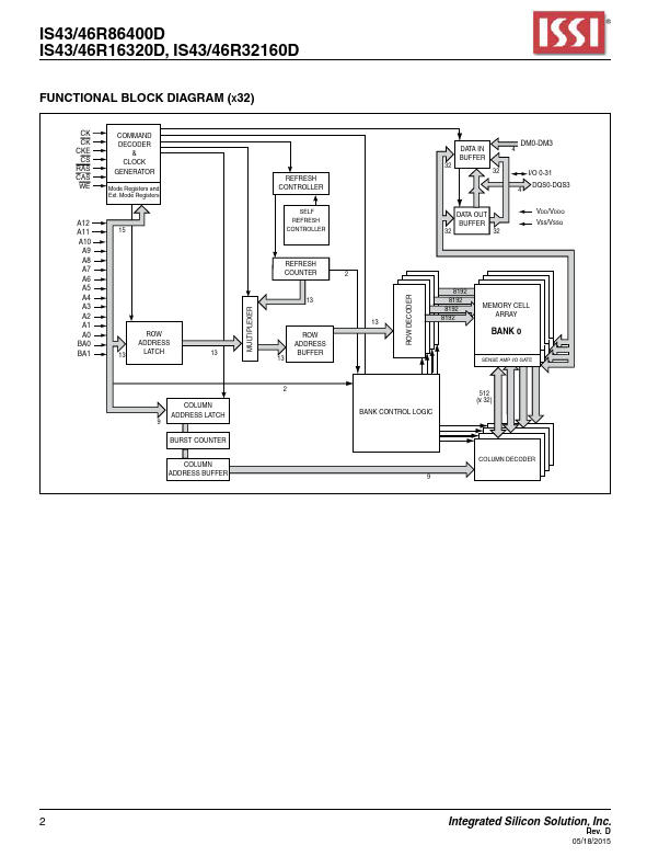
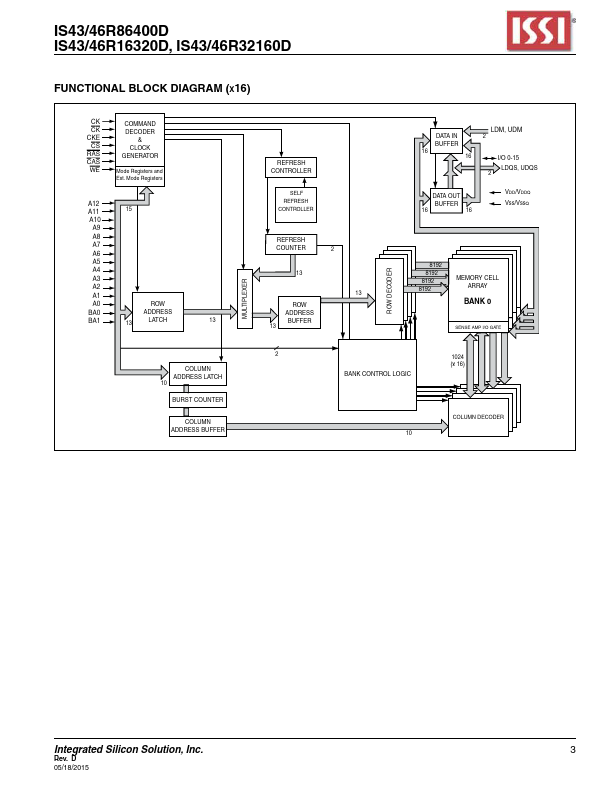
Description
x8
A0-A12 A0-A9, A11 BA0, BA1 DQ0
DQ7 CK, CK CKE CS CAS RAS WE Row Address Input Column Address Input Bank Select Address Data I/O System Clock Input Clock Enable Chip Select Column Address Strobe Command Row Address Strobe Command Write Enable DM DQS VDD VDDQ VSS VSSQ VREF NC Data Writ
Features
- VDD and VDDQ: 2.5V ± 0.2V (-6) VDD and VDDQ: 2.6V ± 0.1V (-5) SSTL_2 compatible I/O Double-data rate architecture; two data transfers per clock cycle Bidirectional, data strobe (DQS) is transmitted/ received with data, to be used in capturing data at the receiver DQS is edge-aligned with data for READs and centr.