IS49NLC93200 Description
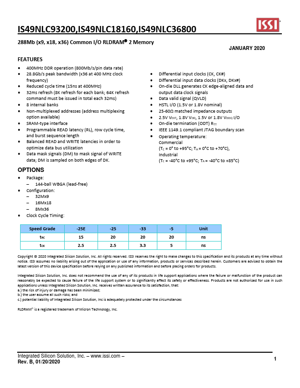
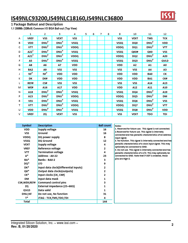
1.1 288Mb (32Mx9) mon I/O BGA Ball-out (Top View) 1 A VREF B VDD C VTT D A221 E A212 F A5 G A8 H BA2 J NF3 K DK L REF# M WE# N A18 P A15 R VSS T VTT U VDD V VREF 2 VSS DNU4 DNU4 DNU4 DNU4 DNU4 A6 A9 NF3 DK# CS# A16 DNU4 DNU4 DNU4 DNU4.
IS49NLC93200 Key Features
- 400MHz DDR operation (800Mb/s/pin data rate)
- 28.8Gb/s peak bandwidth (x36 at 400 MHz clock
- Reduced cycle time (15ns at 400MHz)
- 32ms refresh (8K refresh for each bank; 64K refresh
- 8 internal banks
- Non-multiplexed addresses (address multiplexing
- SRAM-type interface
- Programmable READ latency (RL), row cycle time
- Data mask signals (DM) to mask signal of WRITE
- Package: 144-ball WBGA (lead-free)