IS61NSCS51236
IS61NSCS51236 is Synchronous SRAM manufactured by ISSI.
- Part of the IS61NSCS25672 comparator family.
- Part of the IS61NSCS25672 comparator family.
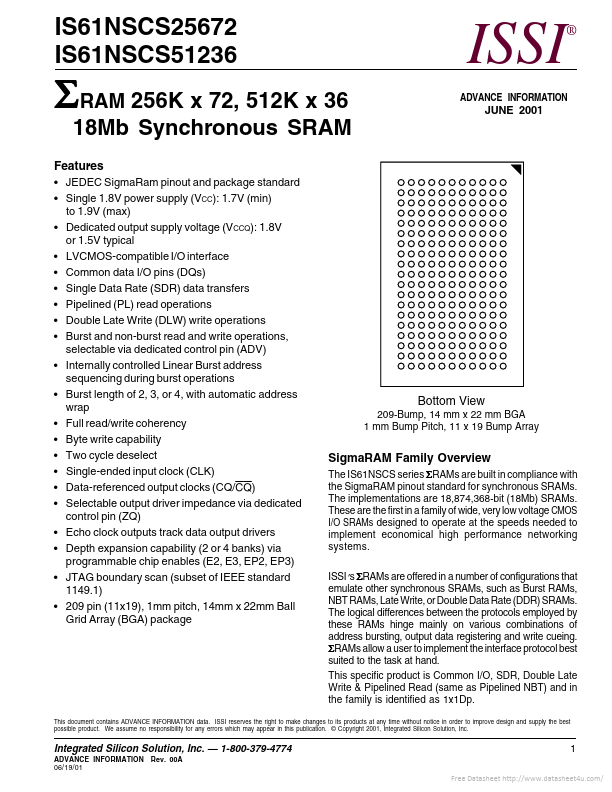
IS61NSCS25672 IS61NSCS51236
Σ RAM 256K x 72, 512K x 36
Features
- JEDEC SigmaRam pinout and package standard
- Single 1.8V power supply (VCC): 1.7V (min) to 1.9V (max)
- Dedicated output supply voltage (VCCQ): 1.8V or 1.5V typical
- LVCMOS-patible I/O interface
- mon data I/O pins (DQs)
- Single Data Rate (SDR) data transfers
- Pipelined (PL) read operations
- Double Late Write (DLW) write operations
- Burst and non-burst read and write operations, selectable via dedicated control pin (ADV)
- Internally controlled Linear Burst address sequencing during burst operations
- Burst length of 2, 3, or 4, with automatic address wrap
- Full read/write coherency
- Byte write capability
- Two...