IS42S16128
IS42S16128 is 128K words x 16 Bits x 2 Banks SDRAM manufactured by ISSI.
128K Words x 16 Bits x 2 Banks (4-MBIT) SYNCHRONOUS DYNAMIC RAM
Features
- Clock frequency: 125 MHz, 100 MHz, 83 MHz
- Two banks can be operated simultaneously and independently
- Single 3.3V power supply
- LVTTL interface
- Programmable burst length
- (1, 2, 4, 8, full page)
- Programmable burst sequence: Sequential/Interleave
- Auto refresh, self refresh
- 1K refresh cycles every 16 ms
- Random column address every clock cycle
- Programmable CAS latency (2, 3 clocks)
- Burst read/write and burst read/single write operations capability
- Byte controlled by LDQM and UDQM
- Package 400-mil 50-pin TSOP II
ISSI
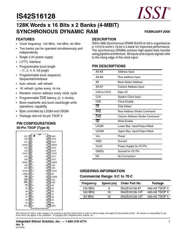
DESCRIPTION PIN DESCRIPTIONS
A0-A9 A0-A8 A9 A0-A7 I/O0 to I/O15 CLK...