Intel Corporation 80188
the 80188 3 3 DataSheet 4 U .com 80186 80188 Leads Facing Up Leads Facing Down 272430 – 4 Figure 4 Plastic Leaded Chip Carrier NOTE Pin names in parentheses apply to the 80188 4 4 DataSheet 4 U .com 80186 80188 Table 1 Pin Descriptions Symbol VCC VSS RESET Pin No 9 43 26 60 57 Type I I O Name and Function SYSTEM POWER a 5 volt power supply System Ground Reset Output indicates that the CPU is being reset and can be used as a system reset It is active HIGH synchronized with the processor clock and lasts an integer number of clock periods corresponding to the length of the RES signal Crystal...| Part No. | 80188 |
|---|---|
| Datasheet | 80188 Download |
| Manufacturer |  Intel Corporation |
| Description | HIGH-INTEGRATION 16-BIT MICROPROCESSORS |
| Buy | Stock & Price |
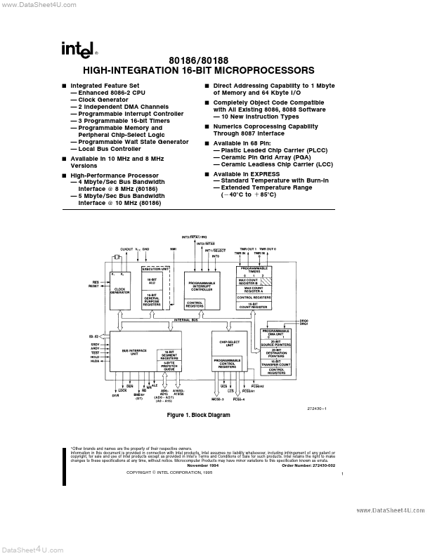
DESCRIPTION
Introduction CLOCK GENERATOR Oscillator Clock Generator READY Synchronization RESET Logic LOCAL BUS CONTROLLER Memory Peripheral Control Local Bus Arbitration Local Bus Controller and Reset PERIPHERAL ARCHITECTURE Chip-Select Ready Generation Logic DMA Channels Timers Interrupt Controller PAGE 9 9 9 9 9 9 9 9 10 10 10 10 10 11 11 12 CONTENTSABSOLUTE MAXIMUM RATINGS
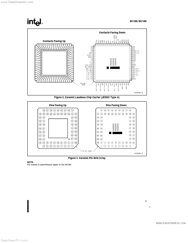
D C CHARACTERISTICS A C CHARACTERISTICS EXPLANATION OF THE AC SYMBOLS WAVEFORMS EXPRESS EXECUTION TIMINGS INSTRUCTION SET SUMMARY FOOTNOTES REVISION HISTORY PAGE 15 15 16 18 19 25 26 27 32 33 2 2 DataSheet 4 U .com 80186 80188 Contacts Facing Down Contacts Facing Up 272430 – 2 Figure 2 Ceramic Leadless Chip Carrier (JEDEC Type A) Pins Facing Up Pins Facing Down 272430 – 3 Figure 3 Ceramic Pin Grid Array NOTE Pin names in parentheses apply to the 80188 3 3 DataSheet 4 U .com 80186 80188 Leads Facing Up Leads Facing Down 272430 – 4 Figure 4 Plastic Leaded Chip Carrier NOTE Pin names in parentheses apply to the 801...