DESCRIPTION
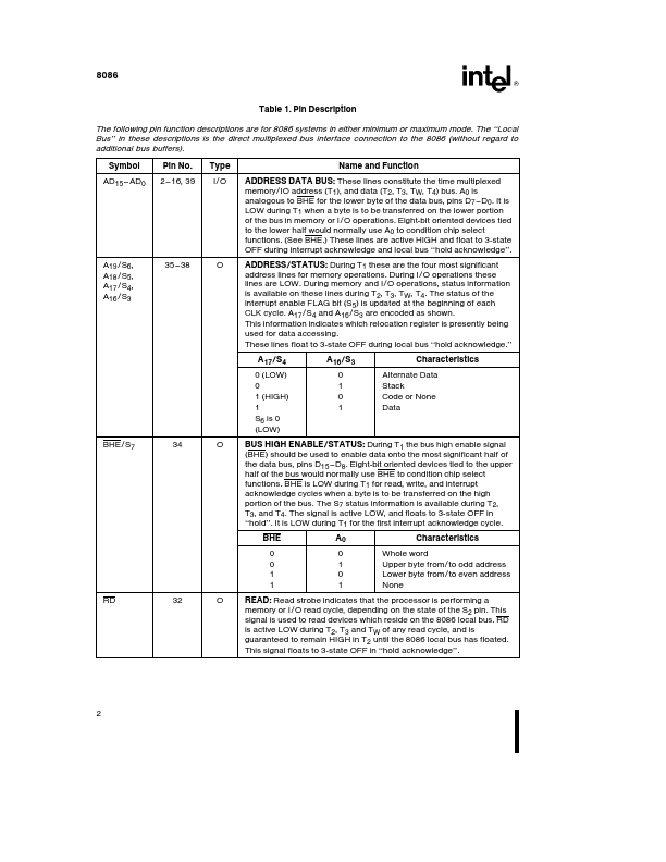
The following pin function descriptions are for 8086 systems in either minimum or maximum mode. Symbol AD15 – AD0 A19/S6, A18/S5, A17/S4, A16/S3 BHE/S7 RD Pin No. 2–16, 39 35 – 38 34 32 Type I/O O O O Name and Function ADDRESS DATA BUS: These lines constitute the time multiplexed memory/IO address (T1), and data (T2, T3, TW, T4) bus. A0 is analogous to BHE for the lower byte of the data bus, pins D7 – D0. It is LOW during T1 when a byte is to be transferred on the lower portion of the bus in memory or I/O operations. Eight-bit oriented devices tied to the lower half would normally use A0 to condition chip select functions. (See BHE.) These lines are active HIGH and float to 3-state OFF during interrupt acknowledge and local bus ‘‘hold acknowledge’’. ADDRESS/STATUS: During T1 these are the four most significant address lines for memory operations. During I/O operations these lines are LOW. During memory and I/O operations, status information is available on these lines during T2, T3, TW, T4. Intel