InterFET J270
The J270 has a cutoff voltage of less than 2.0V ideal for low-level power supplies.| Part No. | J270 |
|---|---|
| Datasheet | J270 Download |
| Manufacturer |  InterFET |
| Description | P-Channel JFET |
| Buy | Stock & Price |
FEATURES
● InterFET P0099F Geometry● Low Noise: 6 nV/√Hz Typical
● RoHS Compliant
● SMT, TH, and Bare Die Package options.
APPLICATIONS
● Analog Switch● Sample and Hold
● Low Noise, High Gain Amplifier
DESCRIPTION
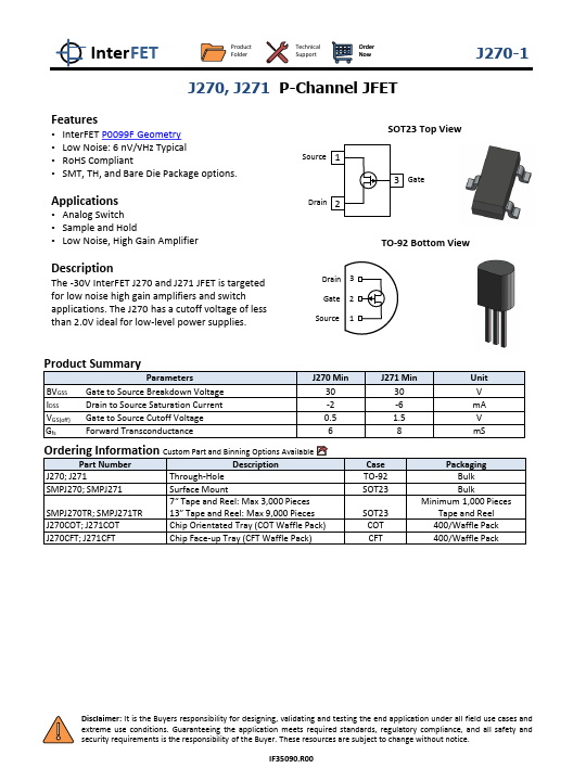
The -30V InterFET J270 and J271 JFET is targeted for low noise high gain amplifiers and switch applications. Source 1 Drain 2 SOT23 Top View 3 Gate TO-92 Bottom View Drain 3 Gate 2 Source 1 Product Summary Parameters BVGSS Gate to Source Breakdown Voltage IDSS Drain to Source Saturation Current VGS(off) Gate to Source Cutoff Voltage Gfs Forward Transconductance J270 Min 30 -2 0.5 6 Ordering Information Custom Part and Binning Options Available Part NumberDESCRIPTION
J270; J271 Through-Hole SMPJ270; SMPJ271 Surface Mount 7“ Tape and Reel: Max 3,000 Pieces SMPJ270TR; SMPJ271TR 13” Tape and Reel: Max 9,000 Pieces J270COT; J271COT Chip Orientated Tray (COT Waffle Pack) J270CFT; J271CFT Chip Face-up Tray (CFT Waffle Pack) J271 Min Unit 30 V -6 mA 1.5 V 8 mS Case TO-92 SOT23 SOT...