InterFET N0072S
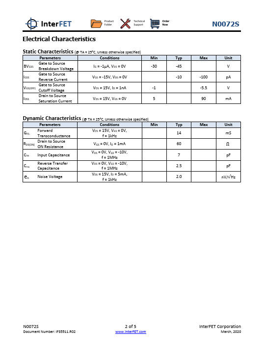
the N0072L Geometry with higher breakdown voltage.| Part No. | N0072S |
|---|---|
| Datasheet | N0072S Download |
| Manufacturer |  InterFET |
| Description | Process Geometry |
| Buy | Stock & Price |
FEATURES
● Low Noise: 2.0 nV/√Hz Typical● Typical Input Capacitance: 6.5pF
● Typical Breakdown Voltage: -45V
● Small Die: 467um X 467um X 203um
● Bond Pads: 90um X 90um
● Substrate Connected to Gate
● Au Back-Side Finish
APPLICATIONS
● Low Noise Amplifier● Audio Amplifiers
● Matched Pair
APPLICATIONS
● Custom Part OptionsDESCRIPTION
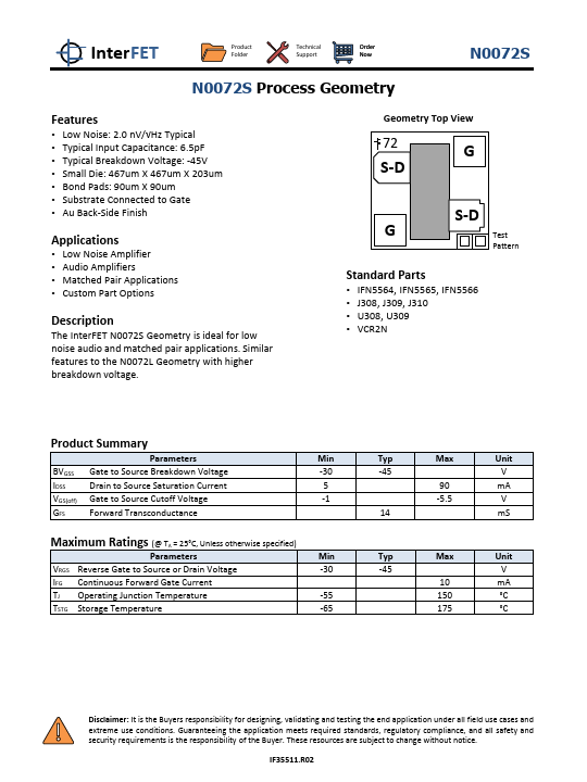
The InterFET N0072S Geometry is ideal for low noise audio and matched pair applications. Similar features to Geometry Top View 72 G S-D S-D G Test Pattern Standard Parts● IFN5564, IFN5565, IFN5566
● J308, J309, J310
● U308, U309
● VCR2N Product Summary Parameters BVGSS Gate to Source Breakdown Voltage IDSS Drain to Source Saturation Current VGS(off) Gate to Source Cutoff Voltage GFS Forward Transconductance Min Typ Max Unit -30 -45 V 5 90 mA -1 -5.5 V 14 mS
MAXIMUM RATINGS
(@ TA = 25°C, Unless otherwise specified) Parameters Min Typ Max Unit VRGS Reverse Gate to Source or Drain Voltage -30 -45 V IFG Continuous Forward Gate Current 10 mA TJ Operating Jun...