IRF6216
- 94297
SMPS MOSFET
Applications Reset Switch for Active Clamp Reset DC-DC converters
HEXFET® Power MOSFET RDS(on) max ID 0.240Ω@VGS =-10V -2.2A l
VDSS
-150V
Benefits Low Gate to Drain Charge to Reduce Switching Losses l Fully Characterized Capacitance Including Effective COSS to Simplify Design (See App. Note AN1001) l Fully Characterized Avalanche Voltage and Current l
8 7
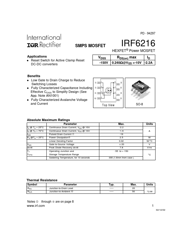
A D D D D
T o p V ie w
SO-8
Absolute Maximum Ratings
Parameter
ID @ TA = 25°C ID @ TA = 70°C IDM PD @TA = 25°C VGS dv/dt TJ TSTG Continuous Drain Current, VGS @ 10V Continuous Drain Current, VGS @ 10V Pulsed Drain Current Power Dissipation- Linear Derating Factor Gate-to-Source Voltage Peak Diode Recovery dv/dt Operating Junction and Storage Temperature Range Soldering Temperature, for 10 seconds
Max.
-2.2 -1.9 -19 2.5 0.02 ± 20 7.8 -55 to + 150 300 (1.6mm from case )
Units
A W W/°C V V/ns °C
Thermal Resistance
Symbol
RθJL RθJA
Parameter
Junction-to-Drain Lead...