IRF7901D1
IRF7901D1 is Dual MOSFET manufactured by International Rectifier.
PD- 93844B
- Co-Pack Dual N-channel HEXFET® Power MOSFET and Schottky Diode
- Ideal for Synchronous Buck DC-DC Converters Up to 5A Peak Output
- Low Conduction Losses
- Low Switching Losses
- Low Vf Schottky Rectifier
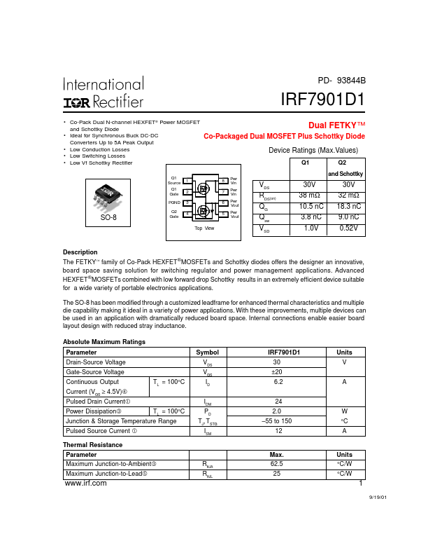
Q1 S ource Q1 Gate PGND 1 2 3 4
Dual FETKY™
Co-Packaged Dual MOSFET Plus Schottky Diode Device Ratings (Max.Values)
Q1
8 7 6 5 Pwr Vin Pwr Vin Pwr Vout Pwr Vout
Q2 and Schottky
VDS RDS(on) QG Qsw VSD
30V 38 mΩ 10.5 nC 3.8 nC 1.0V
30V 32 mΩ 18.3 nC 9.0 nC 0.52V
SO-8
Q2 Gate
T op View
Description The FETKY™ family of Co-Pack HEXFET®MOSFETs and Schottky diodes offers the designer an innovative, board space saving solution for switching regulator and power...