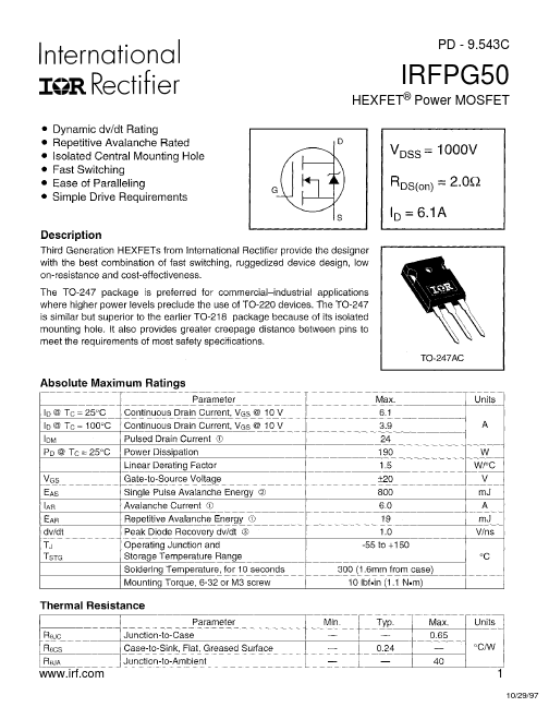
IRFPG50 Description
PD - 9.543C IRFPG50 HEXFET® Power MOSFET .irf. 1 10/29/97 IRFPG50 2 .irf. Maximum Safe Operating Area 4 .irf.
IRFPG50 is Power MOSFET manufactured by International Rectifier.
| Manufacturer | Part Number | Description |
|---|---|---|
| IRFPG50 | Power MOSFET |
PD - 9.543C IRFPG50 HEXFET® Power MOSFET .irf. 1 10/29/97 IRFPG50 2 .irf. Maximum Safe Operating Area 4 .irf.