IRFSL5620PbF
Features
- Key Parameters Optimized for Class-D Audio Amplifier Applications
- Low RDSON for Improved Efficiency
- Low QG and QSW for Better THD and Improved
Efficiency
- Low QRR for Better THD and Lower EMI
- 175°C Operating Junction Temperature for
Ruggedness
- Can Deliver up to 300W per Channel into 8Ω Load in
Half-Bridge Configuration Amplifier
IRFSL5620Pb F
Key Parameters
VDS RDS(ON) typ. @ 10V Qg typ.
200 63.7 25
Qsw typ.
RG(int) typ. TJ max
2.6 175
V m: n C n C
Ω °C
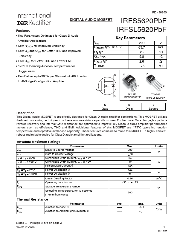
D2Pak
TO-262
S IRFS5620Pb F IRFSL5620Pb F
GD S
Gate
Drain
Source
Description
This Digital Audio MOSFET is specifically designed for Class-D audio amplifier applications. This MOSFET utilizes the latest processing techniques to achieve low on-resistance per silicon area. Furthermore, Gate charge, body-diode reverse recovery and internal Gate resistance are optimized to improve key Class-D audio amplifier performance factors such as efficiency, THD and EMI. Additional...